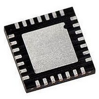
PIC18F26K22-I/ML Microchip Technology, PIC18F26K22-I/ML Datasheet - Page 295

PIC18F26K22-I/ML
Manufacturer Part Number
PIC18F26K22-I/ML
Description
IC PIC MCU 64KB FLASH 28QFN
Manufacturer
Microchip Technology
Series
PIC® XLP™ 18Fr
Datasheets
1.PIC16F722-ISS.pdf
(8 pages)
2.PIC18F26J13-ISS.pdf
(496 pages)
3.PIC18F24K22-ISP.pdf
(494 pages)
Specifications of PIC18F26K22-I/ML
Core Size
8-Bit
Program Memory Size
64KB (32K x 16)
Core Processor
PIC
Speed
64MHz
Connectivity
I²C, SPI, UART/USART
Peripherals
Brown-out Detect/Reset, HLVD, POR, PWM, WDT
Number Of I /o
24
Program Memory Type
FLASH
Eeprom Size
1K x 8
Ram Size
3.8K x 8
Voltage - Supply (vcc/vdd)
1.8 V ~ 5.5 V
Data Converters
A/D 19x10b
Oscillator Type
Internal
Operating Temperature
-40°C ~ 85°C
Package / Case
28-VQFN Exposed Pad
Controller Family/series
PIC18
No. Of I/o's
25
Eeprom Memory Size
1KB
Ram Memory Size
3896Byte
Cpu Speed
64MHz
No. Of Timers
7
Lead Free Status / RoHS Status
Lead free / RoHS Compliant
Available stocks
Company
Part Number
Manufacturer
Quantity
Price
Company:
Part Number:
PIC18F26K22-I/ML
Manufacturer:
MICROCHIP
Quantity:
3 400
Part Number:
PIC18F26K22-I/ML
Manufacturer:
MICROCHIP/微芯
Quantity:
20 000
- Current page: 295 of 494
- Download datasheet (6Mb)
17.1.5
The source of the conversion clock is software
selectable via the ADCS bits of the ADCON2 register.
There are seven possible clock options:
• F
• F
• F
• F
• F
• F
• F
The time to complete one bit conversion is defined as
T
as shown in Figure 17-3.
For correct conversion, the appropriate T
must be met. See A/D conversion requirements in
Table 27-24 for more information. Table gives examples
of appropriate ADC clock selections.
TABLE 17-1:
2010 Microchip Technology Inc.
Legend: Shaded cells are outside of recommended range.
Note 1:
AD
ADC Clock Source
Note:
OSC
OSC
OSC
OSC
OSC
OSC
RC
. One full 10-bit conversion requires 11 T
(dedicated internal oscillator)
F
F
F
2:
3:
4:
/2
/4
/8
/16
/32
/64
F
F
F
OSC
OSC
OSC
OSC
OSC
OSC
F
ADC Clock Period (T
RC
The F
These values violate the minimum required T
For faster conversion times, the selection of another clock source is recommended.
When the device frequency is greater than 1 MHz, the F
conversion will be performed during Sleep.
Unless using the F
system clock frequency will change the
ADC
adversely affect the ADC result.
CONVERSION CLOCK
/16
/32
/64
/2
/4
/8
RC
ADC CLOCK PERIOD (T
clock
source has a typical T
frequency,
ADCS<2:0>
RC
AD
000
100
001
101
010
110
x11
, any changes in the
)
AD
which
specification
AD
AD
time of 1.7 s.
AD
periods
31.25 ns
may
) V
1-4 s
62.5 ns
400 ns
250 ns
500 ns
64 MHz
Preliminary
1.0 s
S
. DEVICE OPERATING FREQUENCIES
(1,4)
AD
(2)
(2)
(2)
(2)
(2)
time.
17.1.6
The ADC module allows for the ability to generate an
interrupt upon completion of an Analog-to-Digital
Conversion. The ADC interrupt enable is the ADIE bit
in the PIE1 register and the interrupt priority is the ADIP
bit in the IPR1 register. The ADC interrupt flag is the
ADIF bit in the PIR1 register. The ADIF bit must be
cleared by software.
This interrupt can be generated while the device is
operating or while in Sleep. If the device is in Sleep, the
interrupt will wake-up the device. Upon waking from
Sleep, the next instruction following the SLEEP
instruction is always executed. If the user is attempting
to wake-up from Sleep and resume in-line code
execution, the global interrupt must be disabled. If the
global interrupt is enabled, execution will switch to the
Interrupt Service Routine.
Note:
PIC18(L)F2X/4XK22
1-4 s
RC
125 ns
250 ns
500 ns
Device Frequency (F
4.0 s
16 MHz
1.0 s
2.0 s
clock source is only recommended if the
(1,4)
(3)
(2)
(2)
(2)
INTERRUPTS
The ADIF bit is set at the completion of
every conversion, regardless of whether
or not the ADC interrupt is enabled.
1-4 s
16.0 s
500 ns
4.0 s
8.0 s
4 MHz
1.0 s
2.0 s
OSC
(1,4)
(3)
(3)
(2)
(3)
)
DS41412A-page 295
1-4 s
16.0 s
32.0 s
64.0 s
4.0 s
8.0 s
1 MHz
2.0 s
(1,4)
(3)
(3)
(3)
(3)
(3)
Related parts for PIC18F26K22-I/ML
Image
Part Number
Description
Manufacturer
Datasheet
Request
R

Part Number:
Description:
Manufacturer:
Microchip Technology Inc.
Datasheet:

Part Number:
Description:
Manufacturer:
Microchip Technology Inc.
Datasheet:

Part Number:
Description:
Manufacturer:
Microchip Technology Inc.
Datasheet:

Part Number:
Description:
Manufacturer:
Microchip Technology Inc.
Datasheet:

Part Number:
Description:
Manufacturer:
Microchip Technology Inc.
Datasheet:

Part Number:
Description:
Manufacturer:
Microchip Technology Inc.
Datasheet:

Part Number:
Description:
Manufacturer:
Microchip Technology Inc.
Datasheet:

Part Number:
Description:
Manufacturer:
Microchip Technology Inc.
Datasheet:


