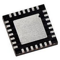
PIC18F26K22-I/ML Microchip Technology, PIC18F26K22-I/ML Datasheet - Page 37

PIC18F26K22-I/ML
Manufacturer Part Number
PIC18F26K22-I/ML
Description
IC PIC MCU 64KB FLASH 28QFN
Manufacturer
Microchip Technology
Series
PIC® XLP™ 18Fr
Datasheets
1.PIC16F722-ISS.pdf
(8 pages)
2.PIC18F26J13-ISS.pdf
(496 pages)
3.PIC18F24K22-ISP.pdf
(494 pages)
Specifications of PIC18F26K22-I/ML
Core Size
8-Bit
Program Memory Size
64KB (32K x 16)
Core Processor
PIC
Speed
64MHz
Connectivity
I²C, SPI, UART/USART
Peripherals
Brown-out Detect/Reset, HLVD, POR, PWM, WDT
Number Of I /o
24
Program Memory Type
FLASH
Eeprom Size
1K x 8
Ram Size
3.8K x 8
Voltage - Supply (vcc/vdd)
1.8 V ~ 5.5 V
Data Converters
A/D 19x10b
Oscillator Type
Internal
Operating Temperature
-40°C ~ 85°C
Package / Case
28-VQFN Exposed Pad
Controller Family/series
PIC18
No. Of I/o's
25
Eeprom Memory Size
1KB
Ram Memory Size
3896Byte
Cpu Speed
64MHz
No. Of Timers
7
Lead Free Status / RoHS Status
Lead free / RoHS Compliant
Available stocks
Company
Part Number
Manufacturer
Quantity
Price
Company:
Part Number:
PIC18F26K22-I/ML
Manufacturer:
MICROCHIP
Quantity:
3 400
Part Number:
PIC18F26K22-I/ML
Manufacturer:
MICROCHIP/微芯
Quantity:
20 000
- Current page: 37 of 494
- Download datasheet (6Mb)
2.5.1.1
The HFINTOSC/MFINTOSC oscillator circuits are
factory calibrated but can be adjusted in software by
writing to the TUN<5:0> bits of the OSCTUNE register
(Register 2-3).
The default value of the TUN<5:0> is ‘000000’. The
value is a 6-bit two’s complement number.
When the OSCTUNE register is modified, the
HFINTOSC/MFINTOSC frequency will begin shifting to
the new frequency. Code execution continues during this
shift. There is no indication that the shift has occurred.
The TUN<5:0> bits in OSCTUNE do not affect the
LFINTOSC frequency. Operation of features that
depend on the LFINTOSC clock source frequency, such
REGISTER 2-3:
2010 Microchip Technology Inc.
bit 7
Legend:
R = Readable bit
-n = Value at POR
bit 7
bit 6
bit 5-0
Note 1:
INTSRC
R/W-0
The PLLEN bit is active only when the HFINTOSC is the primary clock source (FOSC<2:0> = 100X) and
the selected frequency is 8 MHz or 16 MHz (IRCF<2:0> = 11x). Otherwise, the PLLEN bit is unavailable
and always reads ‘0’.
OSCTUNE Register
INTSRC: Internal Oscillator Low-Frequency Source Select bit
1 = 31.25 kHz device clock derived from the MFINTOSC or HFINTOSC source
0 = 31.25 kHz device clock derived directly from LFINTOSC internal oscillator
PLLEN: Frequency Multiplier 4xPLL for HFINTOSC Enable bit
1 = PLL enabled for HFINTOSC (8 MHz and 16 MHz only)
0 = PLL disabled
TUN<5:0>: Frequency Tuning bits – use to adjust MFINTOSC and HFINTOSC frequencies
011111 = Maximum frequency
011110 =
000001 =
000000 = Oscillator module (HFINTOSC and MFINTOSC) are running at the factory calibrated
111111 =
100000 = Minimum frequency
• • •
• • •
PLLEN
R/W-0
OSCTUNE: OSCILLATOR TUNING REGISTER
(1)
frequency.
W = Writable bit
‘1’ = Bit is set
R/W-0
R/W-0
Preliminary
U = Unimplemented bit, read as ‘0’
‘0’ = Bit is cleared
R/W-0
as the Power-up Timer (PWRT), Watchdog Timer
(WDT),
peripherals, are not affected by the change in frequency.
The OSCTUNE register also implements the INTSRC
and PLLEN bits, which control certain features of the
internal oscillator block.
The INTSRC bit allows users to select which internal
oscillator provides the clock source when the
31.25 kHz frequency option is selected. This is covered
in greater detail in Section 2.2.3 “Low Frequency
Selection”.
The PLLEN bit controls the operation of the frequency
multiplier, PLL, in internal oscillator modes. For more
details about the function of the PLLEN bit, see
Section 2.6.2 “PLL in HFINTOSC Modes”
PIC18(L)F2X/4XK22
TUN<5:0>
Fail-Safe
R/W-0
(1)
Clock
x = Bit is unknown
R/W-0
Monitor
DS41412A-page 37
(FSCM)
R/W-0
bit 0
and
Related parts for PIC18F26K22-I/ML
Image
Part Number
Description
Manufacturer
Datasheet
Request
R

Part Number:
Description:
Manufacturer:
Microchip Technology Inc.
Datasheet:

Part Number:
Description:
Manufacturer:
Microchip Technology Inc.
Datasheet:

Part Number:
Description:
Manufacturer:
Microchip Technology Inc.
Datasheet:

Part Number:
Description:
Manufacturer:
Microchip Technology Inc.
Datasheet:

Part Number:
Description:
Manufacturer:
Microchip Technology Inc.
Datasheet:

Part Number:
Description:
Manufacturer:
Microchip Technology Inc.
Datasheet:

Part Number:
Description:
Manufacturer:
Microchip Technology Inc.
Datasheet:

Part Number:
Description:
Manufacturer:
Microchip Technology Inc.
Datasheet:


