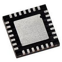
PIC18F26K22-I/ML Microchip Technology, PIC18F26K22-I/ML Datasheet - Page 309

PIC18F26K22-I/ML
Manufacturer Part Number
PIC18F26K22-I/ML
Description
IC PIC MCU 64KB FLASH 28QFN
Manufacturer
Microchip Technology
Series
PIC® XLP™ 18Fr
Datasheets
1.PIC16F722-ISS.pdf
(8 pages)
2.PIC18F26J13-ISS.pdf
(496 pages)
3.PIC18F24K22-ISP.pdf
(494 pages)
Specifications of PIC18F26K22-I/ML
Core Size
8-Bit
Program Memory Size
64KB (32K x 16)
Core Processor
PIC
Speed
64MHz
Connectivity
I²C, SPI, UART/USART
Peripherals
Brown-out Detect/Reset, HLVD, POR, PWM, WDT
Number Of I /o
24
Program Memory Type
FLASH
Eeprom Size
1K x 8
Ram Size
3.8K x 8
Voltage - Supply (vcc/vdd)
1.8 V ~ 5.5 V
Data Converters
A/D 19x10b
Oscillator Type
Internal
Operating Temperature
-40°C ~ 85°C
Package / Case
28-VQFN Exposed Pad
Controller Family/series
PIC18
No. Of I/o's
25
Eeprom Memory Size
1KB
Ram Memory Size
3896Byte
Cpu Speed
64MHz
No. Of Timers
7
Lead Free Status / RoHS Status
Lead free / RoHS Compliant
Available stocks
Company
Part Number
Manufacturer
Quantity
Price
Company:
Part Number:
PIC18F26K22-I/ML
Manufacturer:
MICROCHIP
Quantity:
3 400
Part Number:
PIC18F26K22-I/ML
Manufacturer:
MICROCHIP/微芯
Quantity:
20 000
- Current page: 309 of 494
- Download datasheet (6Mb)
18.2
Each
Configuration register: CM1CON0 for Comparator C1
and CM2CON0 for Comparator C2. In addition,
Comparator C2 has a second control register,
CM2CON1, for controlling the interaction with Timer1 and
simultaneous reading of both comparator outputs.
The CM1CON0 and CM2CON0 registers (see Registers
18-1 and 18-2, respectively) contain the control and
status bits for the following:
• Enable
• Input selection
• Reference selection
• Output selection
• Output polarity
• Speed selection
18.2.1
Setting the CxON bit of the CMxCON0 register enables
the comparator for operation. Clearing the CxON bit
disables the comparator resulting in minimum current
consumption.
18.2.2
The CxCH<1:0> bits of the CMxCON0 register direct
one of four analog input pins to the comparator
inverting input.
18.2.3
Setting the CxR bit of the CMxCON0 register directs an
internal voltage reference or an analog input pin to the
non-inverting
Section 21.0 “Fixed Voltage Reference (FVR)” for
more information on the Internal Voltage Reference
module.
18.2.4
The output of the comparator can be monitored by
reading either the CxOUT bit of the CMxCON0 register
or the MCxOUT bit of the CM2CON1 register. In order
to make the output available for an external connection,
the following conditions must be true:
• CxOE bit of the CMxCON0 register must be set
• Corresponding TRIS bit must be cleared
• CxON bit of the CMxCON0 register must be set
2010 Microchip Technology Inc.
Note:
comparator
Comparator Control
COMPARATOR ENABLE
COMPARATOR INPUT SELECTION
To use CxIN+ and C12INx- pins as analog
inputs, the appropriate bits must be set in
the ANSEL register and the corresponding
TRIS bits must also be set to disable the
output drivers.
COMPARATOR REFERENCE
SELECTION
COMPARATOR OUTPUT
SELECTION
input
has
of
a
the
separate
comparator.
control
See
and
Preliminary
18.2.5
Inverting the output of the comparator is functionally
equivalent to swapping the comparator inputs. The
polarity of the comparator output can be inverted by
setting the CxPOL bit of the CMxCON0 register.
Clearing the CxPOL bit results in a non-inverted output.
Table 18-1 shows the output state versus input
conditions, including polarity control.
TABLE 18-1:
18.2.6
The trade-off between speed or power can be
optimized during program execution with the CxSP
control bit. The default state for this bit is ‘1’ which
selects the normal speed mode. Device power
consumption can be optimized at the cost of slower
comparator propagation delay by clearing the CxSP bit
to ‘0’.
18.3
The comparator output is indeterminate for a period of
time after the change of an input source or the selection
of a new reference voltage. This period is referred to as
the response time. The response time of the
comparator differs from the settling time of the voltage
reference. Therefore, both of these times must be
considered when determining the total response time
to a comparator input change. See the Comparator and
Voltage Reference Specifications in Section 27.0
“Electrical Characteristics” for more details.
Input Condition
CxV
CxV
CxV
CxV
Note 1: The CxOE bit overrides the PORT data
PIC18(L)F2X/4XK22
IN
IN
IN
IN
- > CxV
- < CxV
- > CxV
- < CxV
2: The internal output of the comparator is
Comparator Response Time
COMPARATOR OUTPUT POLARITY
COMPARATOR SPEED SELECTION
latch. Setting the CxON has no impact on
the port override.
latched with each instruction cycle.
Unless otherwise specified, external
outputs are not latched.
IN
IN
IN
IN
+
+
+
+
COMPARATOR OUTPUT
STATE VS. INPUT
CONDITIONS
CxPOL
0
0
1
1
DS41412A-page 309
CxOUT
0
1
1
0
Related parts for PIC18F26K22-I/ML
Image
Part Number
Description
Manufacturer
Datasheet
Request
R

Part Number:
Description:
Manufacturer:
Microchip Technology Inc.
Datasheet:

Part Number:
Description:
Manufacturer:
Microchip Technology Inc.
Datasheet:

Part Number:
Description:
Manufacturer:
Microchip Technology Inc.
Datasheet:

Part Number:
Description:
Manufacturer:
Microchip Technology Inc.
Datasheet:

Part Number:
Description:
Manufacturer:
Microchip Technology Inc.
Datasheet:

Part Number:
Description:
Manufacturer:
Microchip Technology Inc.
Datasheet:

Part Number:
Description:
Manufacturer:
Microchip Technology Inc.
Datasheet:

Part Number:
Description:
Manufacturer:
Microchip Technology Inc.
Datasheet:


