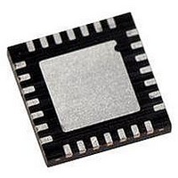
PIC18F26K22-I/ML Microchip Technology, PIC18F26K22-I/ML Datasheet - Page 320

PIC18F26K22-I/ML
Manufacturer Part Number
PIC18F26K22-I/ML
Description
IC PIC MCU 64KB FLASH 28QFN
Manufacturer
Microchip Technology
Series
PIC® XLP™ 18Fr
Datasheets
1.PIC16F722-ISS.pdf
(8 pages)
2.PIC18F26J13-ISS.pdf
(496 pages)
3.PIC18F24K22-ISP.pdf
(494 pages)
Specifications of PIC18F26K22-I/ML
Core Size
8-Bit
Program Memory Size
64KB (32K x 16)
Core Processor
PIC
Speed
64MHz
Connectivity
I²C, SPI, UART/USART
Peripherals
Brown-out Detect/Reset, HLVD, POR, PWM, WDT
Number Of I /o
24
Program Memory Type
FLASH
Eeprom Size
1K x 8
Ram Size
3.8K x 8
Voltage - Supply (vcc/vdd)
1.8 V ~ 5.5 V
Data Converters
A/D 19x10b
Oscillator Type
Internal
Operating Temperature
-40°C ~ 85°C
Package / Case
28-VQFN Exposed Pad
Controller Family/series
PIC18
No. Of I/o's
25
Eeprom Memory Size
1KB
Ram Memory Size
3896Byte
Cpu Speed
64MHz
No. Of Timers
7
Lead Free Status / RoHS Status
Lead free / RoHS Compliant
Available stocks
Company
Part Number
Manufacturer
Quantity
Price
Company:
Part Number:
PIC18F26K22-I/ML
Manufacturer:
MICROCHIP
Quantity:
3 400
Part Number:
PIC18F26K22-I/ML
Manufacturer:
MICROCHIP/微芯
Quantity:
20 000
- Current page: 320 of 494
- Download datasheet (6Mb)
PIC18(L)F2X/4XK22
19.1
The CTMU works by using a fixed current source to
charge a circuit. The type of circuit depends on the type
of measurement being made. In the case of charge
measurement, the current is fixed, and the amount of
time the current is applied to the circuit is fixed. The
amount of voltage read by the A/D is then a measure-
ment of the capacitance of the circuit. In the case of
time measurement, the current, as well as the capaci-
tance of the circuit, is fixed. In this case, the voltage
read by the A/D is then representative of the amount of
time elapsed from the time the current source starts
and stops charging the circuit.
If the CTMU is being used as a time delay, both
capacitance and current source are fixed, as well as the
voltage supplied to the comparator circuit. The delay of
a signal is determined by the amount of time it takes the
voltage to charge to the comparator threshold voltage.
19.1.1
The operation of the CTMU is based on the equation
for charge:
More simply, the amount of charge measured in
coulombs in a circuit is defined as current in amperes
(I) multiplied by the amount of time in seconds that the
current flows (t). Charge is also defined as the
capacitance in farads (C) multiplied by the voltage of
the circuit (V). It follows that:
The CTMU module provides a constant, known current
source. The A/D Converter is used to measure (V) in
the equation, leaving two unknowns: capacitance (C)
and time (t). The above equation can be used to calcu-
late capacitance or time, by either the relationship
using the known fixed capacitance of the circuit:
or by:
using a fixed time that the current source is applied to
the circuit.
DS41412A-page 320
CTMU Operation
THEORY OF OPERATION
C
C
t
I t
=
=
=
I
=
C V
I t
dV
------ -
dT
C V.
V
I
Preliminary
19.1.2
At the heart of the CTMU is a precision current source,
designed to provide a constant reference for measure-
ments. The level of current is user-selectable across
three ranges or a total of two orders of magnitude, with
the ability to trim the output in ±2% increments
(nominal). The current range is selected by the
IRNG<1:0> bits (CTMUICON<1:0>), with a value of
‘00’ representing the lowest range.
Current trim is provided by the ITRIM<5:0> bits
(CTMUICON<7:2>). These six bits allow trimming of
the current source in steps of approximately 2% per
step. Note that half of the range adjusts the current
source positively and the other half reduces the current
source. A value of ‘000000’ is the neutral position (no
change). A value of ‘100000’ is the maximum negative
adjustment (approximately -62%) and ‘011111’ is the
maximum positive adjustment (approximately +62%).
19.1.3
CTMU measurements are controlled by edge events
occurring on the module’s two input channels. Each
channel, referred to as Edge 1 and Edge 2, can be con-
figured to receive input pulses from one of the edge
input pins (CTED1 and CTED2) or ECCPx Special
Event Triggers. The input channels are level-sensitive,
responding to the instantaneous level on the channel
rather than a transition between levels. The inputs are
selected using the EDG1SEL and EDG2SEL bit pairs
(CTMUCONL<3:2 and 6:5>).
In addition to source, each channel can be configured for
event polarity using the EDGE2POL and EDGE1POL
bits (CTMUCONL<7,4>). The input channels can also
be filtered for an edge event sequence (Edge 1 occur-
ring before Edge 2) by setting the EDGSEQEN bit
(CTMUCONH<2>).
19.1.4
The CTMUCONL register also contains two Status bits:
EDG2STAT and EDG1STAT (CTMUCONL<1:0>).
Their primary function is to show if an edge response
has occurred on the corresponding channel. The
CTMU automatically sets a particular bit when an edge
response is detected on its channel. The level-sensitive
nature of the input channels also means that the Status
bits become set immediately if the channel’s configura-
tion is changed and is the same as the channel’s
current state.
CURRENT SOURCE
EDGE SELECTION AND CONTROL
EDGE STATUS
2010 Microchip Technology Inc.
Related parts for PIC18F26K22-I/ML
Image
Part Number
Description
Manufacturer
Datasheet
Request
R

Part Number:
Description:
Manufacturer:
Microchip Technology Inc.
Datasheet:

Part Number:
Description:
Manufacturer:
Microchip Technology Inc.
Datasheet:

Part Number:
Description:
Manufacturer:
Microchip Technology Inc.
Datasheet:

Part Number:
Description:
Manufacturer:
Microchip Technology Inc.
Datasheet:

Part Number:
Description:
Manufacturer:
Microchip Technology Inc.
Datasheet:

Part Number:
Description:
Manufacturer:
Microchip Technology Inc.
Datasheet:

Part Number:
Description:
Manufacturer:
Microchip Technology Inc.
Datasheet:

Part Number:
Description:
Manufacturer:
Microchip Technology Inc.
Datasheet:


