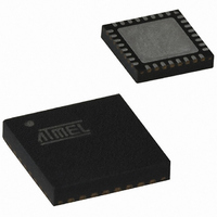
ATTINY261-20MUR Atmel, ATTINY261-20MUR Datasheet - Page 118

ATTINY261-20MUR
Manufacturer Part Number
ATTINY261-20MUR
Description
IC MCU AVR 2K FLASH 20MHZ 32QFN
Manufacturer
Atmel
Series
AVR® ATtinyr
Specifications of ATTINY261-20MUR
Core Processor
AVR
Core Size
8-Bit
Speed
20MHz
Connectivity
USI
Peripherals
Brown-out Detect/Reset, POR, PWM, WDT
Number Of I /o
16
Program Memory Size
2KB (1K x 16)
Program Memory Type
FLASH
Eeprom Size
128 x 8
Ram Size
128 x 8
Voltage - Supply (vcc/vdd)
2.7 V ~ 5.5 V
Data Converters
A/D 11x10b
Oscillator Type
Internal
Operating Temperature
-40°C ~ 85°C
Package / Case
32-VFQFN Exposed Pad
Lead Free Status / RoHS Status
Lead free / RoHS Compliant
- Current page: 118 of 242
- Download datasheet (5Mb)
12.12.4
118
ATtiny261/461/861
TCCR1D – Timer/Counter1 Control Register D
Table 12-20
set to Phase and Frequency Correct PWM Mode.
Table 12-20. Compare Output Mode, Phase and Frequency Correct PWM Mode
• Bit 1 – FOC1D: Force Output Compare Match 1D
The FOC1D bit is only active when the PWM1D bit specify a non-PWM mode.
Writing a logical one to this bit forces a change in the Waveform Output (OCW1D) and the Out-
put Compare pin (OC1D) according to the values already set in COM1D1 and COM1D0. If
COM1D1 and COM1D0 written in the same cycle as FOC1D, the new settings will be used. The
Force Output Compare bit can be used to change the output pin value regardless of the timer
value. The automatic action programmed in COM1D1 and COM1D0 takes place as if a compare
match had occurred, but no interrupt is generated. The FOC1D bit is always read as zero.
• Bit 0 – PWM1D: Pulse Width Modulator D Enable
When set (one) this bit enables PWM mode based on comparator OCR1D.
• Bit 7 – FPIE1: Fault Protection Interrupt Enable
Setting this bit (to one) enables the Fault Protection Interrupt.
• Bit 6 – FPEN1: Fault Protection Mode Enable
Setting this bit (to one) activates the Fault Protection Mode.
• Bit 5 – FPNC1: Fault Protection Noise Canceler
Setting this bit activates the Fault Protection Noise Canceler. When the noise canceler is acti-
vated, the input from the Fault Protection Pin (INT0) is filtered. The filter function requires four
successive equal valued samples of the INT0 pin for changing its output. The Fault Protection is
therefore delayed by four Oscillator cycles when the noise canceler is enabled.
• Bit 4 – FPES1: Fault Protection Edge Select
This bit selects which edge on the Fault Protection pin (INT0) is used to trigger a fault event.
When the FPES1 bit is written to zero, a falling (negative) edge is used as trigger, and when the
FPES1 bit is written to one, a rising (positive) edge will trigger the fault.
Bit
0x26 (0x46)
Read/Write
Initial value
COM1D1:0
00
01
10
11
shows the COM1D1:0 bit functionality when the PWM1D and WGM11:10 bits are
FPIE1
OCW1D Behaviour
Normal port operation.
Cleared on Compare Match when up-counting.
Set on Compare Match when down-counting.
Cleared on Compare Match when up-counting.
Set on Compare Match when down-counting.
Set on Compare Match when up-counting.
Cleared on Compare Match when down-counting.
R/W
7
0
FPEN1
R/W
6
0
FPNC1
R/W
5
0
FPES1
R/W
4
0
FPAC1
R/W
3
0
FPF1
R/W
2
0
OC1D Pin
Disconnected
Connected
Connected
Connected
WGM11
R/W
1
0
WGM10
R/W
OC1D Pin
Disconnected
Connected
Disconnected
Disconnected
0
0
2588E–AVR–08/10
TCCR1D
Related parts for ATTINY261-20MUR
Image
Part Number
Description
Manufacturer
Datasheet
Request
R

Part Number:
Description:
Manufacturer:
Atmel Corporation
Datasheet:

Part Number:
Description:
Manufacturer:
Atmel Corporation
Datasheet:

Part Number:
Description:
IC MCU AVR 2K FLASH 20MHZ 32-QFN
Manufacturer:
Atmel
Datasheet:

Part Number:
Description:
IC MCU AVR 2K FLASH 20MHZ 20-DIP
Manufacturer:
Atmel
Datasheet:

Part Number:
Description:
MCU AVR 2K FLASH 15MHZ 32-QFN
Manufacturer:
Atmel
Datasheet:

Part Number:
Description:
MCU AVR 2KB FLASH 15MHZ 32-VQFN
Manufacturer:
Atmel
Datasheet:

Part Number:
Description:
IC MCU AVR 2K FLASH 20MHZ 20SOIC
Manufacturer:
Atmel
Datasheet:

Part Number:
Description:
Attiny261 8-bit Microcontroller With 2/4/8k Bytes In-system Programmable Flash
Manufacturer:
ATMEL Corporation
Datasheet:

Part Number:
Description:
IC MCU AVR 2K FLASH 20MHZ 20SOIC
Manufacturer:
Atmel
Datasheet:

Part Number:
Description:
Manufacturer:
Atmel Corporation
Datasheet:


