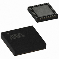
ATTINY261-20MUR Atmel, ATTINY261-20MUR Datasheet - Page 77

ATTINY261-20MUR
Manufacturer Part Number
ATTINY261-20MUR
Description
IC MCU AVR 2K FLASH 20MHZ 32QFN
Manufacturer
Atmel
Series
AVR® ATtinyr
Specifications of ATTINY261-20MUR
Core Processor
AVR
Core Size
8-Bit
Speed
20MHz
Connectivity
USI
Peripherals
Brown-out Detect/Reset, POR, PWM, WDT
Number Of I /o
16
Program Memory Size
2KB (1K x 16)
Program Memory Type
FLASH
Eeprom Size
128 x 8
Ram Size
128 x 8
Voltage - Supply (vcc/vdd)
2.7 V ~ 5.5 V
Data Converters
A/D 11x10b
Oscillator Type
Internal
Operating Temperature
-40°C ~ 85°C
Package / Case
32-VFQFN Exposed Pad
Lead Free Status / RoHS Status
Lead free / RoHS Compliant
- Current page: 77 of 242
- Download datasheet (5Mb)
11.6.1
11.6.2
11.7
Table 11-3.
2588E–AVR–08/10
Mode
0
1
2
3
4
Modes of Operation
Compare Match Blocking by TCNT0 Write
Using the Output Compare Unit
ICEN0
0
0
0
1
1
Modes of operation
TCW0
0
0
1
0
1
OCF0B, but in 16-bit mode the match can set only the Output Compare Flag OCF0A as there is
only one Output Compare Unit. If the corresponding interrupt is enabled, the Output Compare
Flag generates an Output Compare interrupt. The Output Compare Flag is automatically cleared
when the interrupt is executed. Alternatively, the flag can be cleared by software by writing a log-
ical one to its I/O bit location.
Figure 11-5. Output Compare Unit, Block Diagram
All CPU write operations to the TCNT0H/L Register will block any Compare Match that occur in
the next timer clock cycle, even when the timer is stopped. This feature allows OCR0A/B to be
initialized to the same value as TCNT0 without triggering an interrupt when the Timer/Counter
clock is enabled.
Since writing TCNT0H/L will block all Compare Matches for one timer clock cycle, there are risks
involved when changing TCNT0H/L when using the Output Compare Unit, independently of
whether the Timer/Counter is running or not. If the value written to TCNT0H/L equals the
OCR0A/B value, the Compare Match will be missed.
The mode of operation, i.e., the behavior of the Timer/Counter and the Output Compare pins, is
defined by the Timer/Counter Width (TCW0), Input Capture Enable (ICEN0) and Wave Genera-
tion Mode (CTC0) bits. See
Table 11-3
CTC0
X
X
X
0
1
summarises the different modes of operation.
Mode of Operation
Normal, 8-bit Mode
CTC Mode, 8-bit
Normal, 16-bit Mode
Input Capture Mode, 8-bit
Input Capture Mode, 16-bit
OCRnx
“TCCR0A – Timer/Counter0 Control Register A” on page
Figure 11-5
=
(8/16-bit Comparator )
DATA BUS
OCFnx (Int.Req.)
shows a block diagram of the Output Compare unit.
0xFFFF
0xFFFF
OCR0A
0xFF
0xFF
TOP
Update of OCRx at
Immediate
Immediate
Immediate
Immediate
Immediate
TCNTn
TOV Flag Set on
MAX (0xFFFF)
MAX (0xFFFF)
MAX (0xFF)
MAX (0xFF)
MAX (0xFF)
84.
77
Related parts for ATTINY261-20MUR
Image
Part Number
Description
Manufacturer
Datasheet
Request
R

Part Number:
Description:
Manufacturer:
Atmel Corporation
Datasheet:

Part Number:
Description:
Manufacturer:
Atmel Corporation
Datasheet:

Part Number:
Description:
IC MCU AVR 2K FLASH 20MHZ 32-QFN
Manufacturer:
Atmel
Datasheet:

Part Number:
Description:
IC MCU AVR 2K FLASH 20MHZ 20-DIP
Manufacturer:
Atmel
Datasheet:

Part Number:
Description:
MCU AVR 2K FLASH 15MHZ 32-QFN
Manufacturer:
Atmel
Datasheet:

Part Number:
Description:
MCU AVR 2KB FLASH 15MHZ 32-VQFN
Manufacturer:
Atmel
Datasheet:

Part Number:
Description:
IC MCU AVR 2K FLASH 20MHZ 20SOIC
Manufacturer:
Atmel
Datasheet:

Part Number:
Description:
Attiny261 8-bit Microcontroller With 2/4/8k Bytes In-system Programmable Flash
Manufacturer:
ATMEL Corporation
Datasheet:

Part Number:
Description:
IC MCU AVR 2K FLASH 20MHZ 20SOIC
Manufacturer:
Atmel
Datasheet:

Part Number:
Description:
Manufacturer:
Atmel Corporation
Datasheet:


