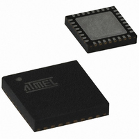
ATTINY261-20MUR Atmel, ATTINY261-20MUR Datasheet - Page 98

ATTINY261-20MUR
Manufacturer Part Number
ATTINY261-20MUR
Description
IC MCU AVR 2K FLASH 20MHZ 32QFN
Manufacturer
Atmel
Series
AVR® ATtinyr
Specifications of ATTINY261-20MUR
Core Processor
AVR
Core Size
8-Bit
Speed
20MHz
Connectivity
USI
Peripherals
Brown-out Detect/Reset, POR, PWM, WDT
Number Of I /o
16
Program Memory Size
2KB (1K x 16)
Program Memory Type
FLASH
Eeprom Size
128 x 8
Ram Size
128 x 8
Voltage - Supply (vcc/vdd)
2.7 V ~ 5.5 V
Data Converters
A/D 11x10b
Oscillator Type
Internal
Operating Temperature
-40°C ~ 85°C
Package / Case
32-VFQFN Exposed Pad
Lead Free Status / RoHS Status
Lead free / RoHS Compliant
- Current page: 98 of 242
- Download datasheet (5Mb)
98
ATtiny261/461/861
Figure 12-10. Compare Match Output Unit, Schematic
The general I/O port function is overridden by the Output Compare (OC1x / OC1x) from the
Dead Time Generator if either of the COM1x1:0 bits are set. However, the OC1x pin direction
(input or output) is still controlled by the Data Direction Register (DDR) for the port pin. The Data
Direction Register bit for the OC1x and OC1x pins (DDR_OC1x and DDR_OC1x) must be set as
output before the OC1x and OC1x values are visible on the pin. The port override function is
independent of the Output Compare mode.
clk I/O
PORTB0
DDRB0
PORTB1
DDRB1
PORTB2
DDRB2
PORTB3
DDRB3
PORTB4
DDRB4
PORTB5
DDRB5
D Q
D Q
D Q
D Q
D Q
D Q
D Q
D Q
D Q
D Q
D Q
D Q
OCW1A
clk Tn
OCW1B
OCW1D
clk Tn
clk Tn
Generator A
Generator B
Generator D
Dead Time
Dead Time
Dead Time
WGM11
OC1OE1:0
COM1A1:0
WGM11
OC1OE3:2
COM1B1:0
WGM11
OC1OE5:4
COM1D1:0
Q
Q
Q
Q
Q
Q
OC1B
OC1B
OC1A
OC1A
OC1D
OC1D
0
1
Output Compare
Pin Configuration
2
1
0
2
1
0
Output Compare
Pin Configuration
Output Compare
Pin Configuration
1
0
1
0
1
0
1
0
1
0
1
0
1
0
1
0
2588E–AVR–08/10
OC1A
OC1A
OC1B
OC1B
OC1D
OC1D
PIN
PIN
PIN
PIN
PIN
PIN
Related parts for ATTINY261-20MUR
Image
Part Number
Description
Manufacturer
Datasheet
Request
R

Part Number:
Description:
Manufacturer:
Atmel Corporation
Datasheet:

Part Number:
Description:
Manufacturer:
Atmel Corporation
Datasheet:

Part Number:
Description:
IC MCU AVR 2K FLASH 20MHZ 32-QFN
Manufacturer:
Atmel
Datasheet:

Part Number:
Description:
IC MCU AVR 2K FLASH 20MHZ 20-DIP
Manufacturer:
Atmel
Datasheet:

Part Number:
Description:
MCU AVR 2K FLASH 15MHZ 32-QFN
Manufacturer:
Atmel
Datasheet:

Part Number:
Description:
MCU AVR 2KB FLASH 15MHZ 32-VQFN
Manufacturer:
Atmel
Datasheet:

Part Number:
Description:
IC MCU AVR 2K FLASH 20MHZ 20SOIC
Manufacturer:
Atmel
Datasheet:

Part Number:
Description:
Attiny261 8-bit Microcontroller With 2/4/8k Bytes In-system Programmable Flash
Manufacturer:
ATMEL Corporation
Datasheet:

Part Number:
Description:
IC MCU AVR 2K FLASH 20MHZ 20SOIC
Manufacturer:
Atmel
Datasheet:

Part Number:
Description:
Manufacturer:
Atmel Corporation
Datasheet:


