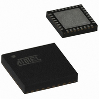
ATTINY261-20MUR Atmel, ATTINY261-20MUR Datasheet - Page 53

ATTINY261-20MUR
Manufacturer Part Number
ATTINY261-20MUR
Description
IC MCU AVR 2K FLASH 20MHZ 32QFN
Manufacturer
Atmel
Series
AVR® ATtinyr
Specifications of ATTINY261-20MUR
Core Processor
AVR
Core Size
8-Bit
Speed
20MHz
Connectivity
USI
Peripherals
Brown-out Detect/Reset, POR, PWM, WDT
Number Of I /o
16
Program Memory Size
2KB (1K x 16)
Program Memory Type
FLASH
Eeprom Size
128 x 8
Ram Size
128 x 8
Voltage - Supply (vcc/vdd)
2.7 V ~ 5.5 V
Data Converters
A/D 11x10b
Oscillator Type
Internal
Operating Temperature
-40°C ~ 85°C
Package / Case
32-VFQFN Exposed Pad
Lead Free Status / RoHS Status
Lead free / RoHS Compliant
- Current page: 53 of 242
- Download datasheet (5Mb)
9.3.3
2588E–AVR–08/10
GIFR – General Interrupt Flag Register
Control Register (MCUCR) define whether the external interrupt is activated on rising and/or fall-
ing edge of the INT0 pin or level sensed. Activity on the pin will cause an interrupt request even
if INT0 is configured as an output. The corresponding interrupt of External Interrupt Request 0 is
executed from the INT0 Interrupt Vector.
• Bit 5 – PCIE1: Pin Change Interrupt Enable
When the PCIE1 bit is set (one) and the I-bit in the Status Register (SREG) is set (one), pin
change interrupt is enabled. Any change on any enabled PCINT7:0 or PCINT15:12 pin will
cause an interrupt. The corresponding interrupt of Pin Change Interrupt Request is executed
from the PCI Interrupt Vector. PCINT7:0 and PCINT15:12 pins are enabled individually by the
PCMSK0 and PCMSK1 Register.
• Bit 4 – PCIE0: Pin Change Interrupt Enable
When the PCIE0 bit is set (one) and the I-bit in the Status Register (SREG) is set (one), pin
change interrupt is enabled. Any change on any enabled PCINT11:8 pin will cause an interrupt.
The corresponding interrupt of Pin Change Interrupt Request is executed from the PCI Interrupt
Vector. PCINT11:8 pins are enabled individually by the PCMSK1 Register.
• Bits 3:0 – Res: Reserved Bits
These bits are reserved and will always read as zero.
• Bit 7 – INTF1: External Interrupt Flag 1
When an edge or logic change on the INT1 pin triggers an interrupt request, INTF1 becomes set
(one). If the I-bit in SREG and the INT1 bit in GIMSK are set (one), the MCU will jump to the cor-
responding Interrupt Vector. The flag is cleared when the interrupt routine is executed.
Alternatively, the flag can be cleared by writing a logical one to it. This flag is always cleared
when INT1 is configured as a level interrupt.
• Bit 6 – INTF0: External Interrupt Flag 0
When an edge or logic change on the INT0 pin triggers an interrupt request, INTF0 becomes set
(one). If the I-bit in SREG and the INT0 bit in GIMSK are set (one), the MCU will jump to the cor-
responding Interrupt Vector. The flag is cleared when the interrupt routine is executed.
Alternatively, the flag can be cleared by writing a logical one to it. This flag is always cleared
when INT0 is configured as a level interrupt.
• Bit 5 – PCIF: Pin Change Interrupt Flag
When a logic change on any PCINT15 pin triggers an interrupt request, PCIF becomes set
(one). If the I-bit in SREG and the PCIE bit in GIMSK are set (one), the MCU will jump to the cor-
responding Interrupt Vector. The flag is cleared when the interrupt routine is executed.
Alternatively, the flag can be cleared by writing a logical one to it.
• Bits 4:0 – Res: Reserved Bits
These bits are reserved and will always read as zero.
Bit
0x3A (0x5A)
Read/Write
Initial Value
7
INT1
R/W
0
6
INTF0
R/W
0
5
PCIF
R/W
0
4
–
R
0
3
–
R
0
2
–
R
0
1
–
R
0
0
–
R
0
GIFR
53
Related parts for ATTINY261-20MUR
Image
Part Number
Description
Manufacturer
Datasheet
Request
R

Part Number:
Description:
Manufacturer:
Atmel Corporation
Datasheet:

Part Number:
Description:
Manufacturer:
Atmel Corporation
Datasheet:

Part Number:
Description:
IC MCU AVR 2K FLASH 20MHZ 32-QFN
Manufacturer:
Atmel
Datasheet:

Part Number:
Description:
IC MCU AVR 2K FLASH 20MHZ 20-DIP
Manufacturer:
Atmel
Datasheet:

Part Number:
Description:
MCU AVR 2K FLASH 15MHZ 32-QFN
Manufacturer:
Atmel
Datasheet:

Part Number:
Description:
MCU AVR 2KB FLASH 15MHZ 32-VQFN
Manufacturer:
Atmel
Datasheet:

Part Number:
Description:
IC MCU AVR 2K FLASH 20MHZ 20SOIC
Manufacturer:
Atmel
Datasheet:

Part Number:
Description:
Attiny261 8-bit Microcontroller With 2/4/8k Bytes In-system Programmable Flash
Manufacturer:
ATMEL Corporation
Datasheet:

Part Number:
Description:
IC MCU AVR 2K FLASH 20MHZ 20SOIC
Manufacturer:
Atmel
Datasheet:

Part Number:
Description:
Manufacturer:
Atmel Corporation
Datasheet:


