ATTINY261-20MUR Atmel, ATTINY261-20MUR Datasheet - Page 67
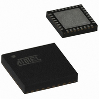
ATTINY261-20MUR
Manufacturer Part Number
ATTINY261-20MUR
Description
IC MCU AVR 2K FLASH 20MHZ 32QFN
Manufacturer
Atmel
Series
AVR® ATtinyr
Specifications of ATTINY261-20MUR
Core Processor
AVR
Core Size
8-Bit
Speed
20MHz
Connectivity
USI
Peripherals
Brown-out Detect/Reset, POR, PWM, WDT
Number Of I /o
16
Program Memory Size
2KB (1K x 16)
Program Memory Type
FLASH
Eeprom Size
128 x 8
Ram Size
128 x 8
Voltage - Supply (vcc/vdd)
2.7 V ~ 5.5 V
Data Converters
A/D 11x10b
Oscillator Type
Internal
Operating Temperature
-40°C ~ 85°C
Package / Case
32-VFQFN Exposed Pad
Lead Free Status / RoHS Status
Lead free / RoHS Compliant


2588E–AVR–08/10
• Port B, Bit 6 – ADC9/ T0/ INT0/ PCINT14
• Port B, Bit 5 – XTAL2/ CLKO/ ADC8/ PCINT13
• Port B, Bit 4 – XTAL1/ CLKI/ OC1B/ ADC7/ PCINT12
• Port B, Bit 3 – OC1B/ PCINT11
• Port B, Bit 2 – SCK/ USCK/ SCL/ OC1B/ PCINT10
• ADC10: ADC input Channel 10. Note that ADC input channel 10 uses analog power.
• PCINT15: Pin Change Interrupt source 15.
• ADC9: ADC input Channel 9. Note that ADC input channel 9 uses analog power.
• T0: Timer/Counter0 counter source.
• INT0: The PB6 pin can serve as an External Interrupt source 0.
• PCINT14: Pin Change Interrupt source 14.
• XTAL2: Chip clock Oscillator pin 2. Used as clock pin for crystal Oscillator or Low-frequency
• CLKO: The divided system clock can be output on the PB5 pin, if the CKOUT Fuse is
• OC1D Output Compare Match output: The PB5 pin can serve as an external output for the
• ADC8: ADC input Channel 8. Note that ADC input channel 8 uses analog power.
• PCINT13: Pin Change Interrupt source 13.
• XTAL1/CLKI: Chip clock Oscillator pin 1. Used for all chip clock sources except internal
• OC1D: Inverted Output Compare Match output: The PB4 pin can serve as an external output
• ADC7: ADC input Channel 7. Note that ADC input channel 7 uses analog power.
• PCINT12: Pin Change Interrupt source 12.
• OC1B, Output Compare Match output: The PB3 pin can serve as an external output for the
• PCINT11: Pin Change Interrupt source 11.
• USCK: Three-wire mode Universal Serial Interface Clock.
• SCL: Two-wire mode Serial Clock for USI Two-wire mode.
• OC1B: Inverted Output Compare Match output: The PB2 pin can serve as an external output
• PCINT10: Pin Change Interrupt source 10.
crystal Oscillator. When used as a clock pin, the pin can not be used as an I/O pin.
programmed, regardless of the PORTB5 and DDB5 settings. It will also be output during
reset.
Timer/Counter1 Compare Match D when configured as an output (DDA1 set). The OC1D pin
is also the output pin for the PWM mode timer function.
calibrated RC Oscillator. When used as a clock pin, the pin can not be used as an I/O pin.
for the Timer/Counter1 Compare Match D when configured as an output (DDA0 set). The
OC1D pin is also the inverted output pin for the PWM mode timer function.
Timer/Counter1 Compare Match B. The PB3 pin has to be configured as an output (DDB3
set (one)) to serve this function. The OC1B pin is also the output pin for the PWM mode timer
function.
for the Timer/Counter1 Compare Match B when configured as an output (DDB2 set). The
OC1B pin is also the inverted output pin for the PWM mode timer function.
67
Related parts for ATTINY261-20MUR
Image
Part Number
Description
Manufacturer
Datasheet
Request
R

Part Number:
Description:
Manufacturer:
Atmel Corporation
Datasheet:
Part Number:
Description:
Manufacturer:
Atmel Corporation
Datasheet:

Part Number:
Description:
IC MCU AVR 2K FLASH 20MHZ 32-QFN
Manufacturer:
Atmel
Datasheet:

Part Number:
Description:
IC MCU AVR 2K FLASH 20MHZ 20-DIP
Manufacturer:
Atmel
Datasheet:

Part Number:
Description:
MCU AVR 2K FLASH 15MHZ 32-QFN
Manufacturer:
Atmel
Datasheet:
Part Number:
Description:
MCU AVR 2KB FLASH 15MHZ 32-VQFN
Manufacturer:
Atmel
Datasheet:

Part Number:
Description:
IC MCU AVR 2K FLASH 20MHZ 20SOIC
Manufacturer:
Atmel
Datasheet:
Part Number:
Description:
Attiny261 8-bit Microcontroller With 2/4/8k Bytes In-system Programmable Flash
Manufacturer:
ATMEL Corporation
Datasheet:

Part Number:
Description:
IC MCU AVR 2K FLASH 20MHZ 20SOIC
Manufacturer:
Atmel
Datasheet:
Part Number:
Description:
Manufacturer:
Atmel Corporation
Datasheet: