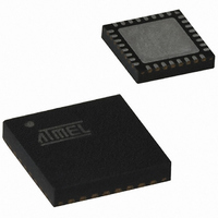
ATTINY261-20MUR Atmel, ATTINY261-20MUR Datasheet - Page 66

ATTINY261-20MUR
Manufacturer Part Number
ATTINY261-20MUR
Description
IC MCU AVR 2K FLASH 20MHZ 32QFN
Manufacturer
Atmel
Series
AVR® ATtinyr
Specifications of ATTINY261-20MUR
Core Processor
AVR
Core Size
8-Bit
Speed
20MHz
Connectivity
USI
Peripherals
Brown-out Detect/Reset, POR, PWM, WDT
Number Of I /o
16
Program Memory Size
2KB (1K x 16)
Program Memory Type
FLASH
Eeprom Size
128 x 8
Ram Size
128 x 8
Voltage - Supply (vcc/vdd)
2.7 V ~ 5.5 V
Data Converters
A/D 11x10b
Oscillator Type
Internal
Operating Temperature
-40°C ~ 85°C
Package / Case
32-VFQFN Exposed Pad
Lead Free Status / RoHS Status
Lead free / RoHS Compliant
- Current page: 66 of 242
- Download datasheet (5Mb)
10.2.2
66
ATtiny261/461/861
Alternate Functions of Port B
The Port B pins with alternate function are shown in
Table 10-6.
• Port B, Bit 7 – RESET/ dW/ ADC10/ PCINT15
• RESET, Reset pin: When the RSTDISBL Fuse is programmed, this pin functions as a normal
• If PB7 is used as a reset pin, DDB7, PORTB7 and PINB7 will all read 0.
• dW: When the debugWIRE Enable (DWEN) Fuse is programmed and Lock bits are
I/O pin, and the part will have to rely on Power-on Reset and Brown-out Reset as its reset
sources. When the RSTDISBL Fuse is unprogrammed, the reset circuitry is connected to the
pin, and the pin can not be used as an I/O pin.
unprogrammed, the RESET port pin is configured as a wire-AND (open-drain) bi-directional
I/O pin with pull-up enabled and becomes the communication gateway between target and
emulator.
Port Pin
PB7
PB6
PB5
PB4
PB3
PB2
PB1
PB0
Port B Pins Alternate Functions
Alternate Function
RESET: Reset pin
dW:
ADC10: ADC Input Channel 10
PCINT15:Pin Change Interrupt 0, Source 15
ADC9:
T0:
INT0:
PCINT14:Pin Change Interrupt 0, Source 14
XTAL2: Crystal Oscillator Output
CLKO: System Clock Output
OC1D: Timer/Counter1 Compare Match D Output
ADC8:
PCINT13:Pin Change Interrupt 0, Source 13
XTAL1: Crystal Oscillator Input
CLKI:
OC1D: Inverted Timer/Counter1 Compare Match D Output
ADC7:
PCINT12:Pin Change Interrupt 0, Source 12
OC1B: Timer/Counter1 Compare Match B Output
PCINT11:Pin Change Interrupt 0, Source 11
USCK: USI Clock (Three Wire Mode)
SCL :
OC1B: Inverted Timer/Counter1 Compare Match B Output
PCINT10:Pin Change Interrupt 0, Source 10
DO:
OC1A: Timer/Counter1 Compare Match A Output
PCINT9: Pin Change Interrupt 1, Source 9
DI:
SDA:
OC1A: Inverted Timer/Counter1 Compare Match A Output
PCINT8: Pin Change Interrupt 1, Source 8
debugWire I/O
ADC Input Channel 9
Timer/Counter0 Clock Source
External Interrupt 0 Input
ADC Input Channel 8
External Clock Input
ADC Input Channel 7
USI Clock (Two Wire Mode)
USI Data Output (Three Wire Mode)
USI Data Input (Three Wire Mode)
USI Data Input (Two Wire Mode)
Table
10-6.
2588E–AVR–08/10
Related parts for ATTINY261-20MUR
Image
Part Number
Description
Manufacturer
Datasheet
Request
R

Part Number:
Description:
Manufacturer:
Atmel Corporation
Datasheet:

Part Number:
Description:
Manufacturer:
Atmel Corporation
Datasheet:

Part Number:
Description:
IC MCU AVR 2K FLASH 20MHZ 32-QFN
Manufacturer:
Atmel
Datasheet:

Part Number:
Description:
IC MCU AVR 2K FLASH 20MHZ 20-DIP
Manufacturer:
Atmel
Datasheet:

Part Number:
Description:
MCU AVR 2K FLASH 15MHZ 32-QFN
Manufacturer:
Atmel
Datasheet:

Part Number:
Description:
MCU AVR 2KB FLASH 15MHZ 32-VQFN
Manufacturer:
Atmel
Datasheet:

Part Number:
Description:
IC MCU AVR 2K FLASH 20MHZ 20SOIC
Manufacturer:
Atmel
Datasheet:

Part Number:
Description:
Attiny261 8-bit Microcontroller With 2/4/8k Bytes In-system Programmable Flash
Manufacturer:
ATMEL Corporation
Datasheet:

Part Number:
Description:
IC MCU AVR 2K FLASH 20MHZ 20SOIC
Manufacturer:
Atmel
Datasheet:

Part Number:
Description:
Manufacturer:
Atmel Corporation
Datasheet:


