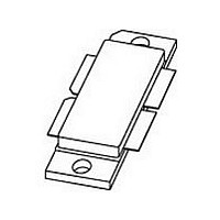
BLF369,112 NXP Semiconductors, BLF369,112 Datasheet - Page 11

BLF369,112
Manufacturer Part Number
BLF369,112
Description
RF MOSFET Small Signal RF LDMOS 65V 100A
Manufacturer
NXP Semiconductors
Datasheet
1.BLF369112.pdf
(17 pages)
Specifications of BLF369,112
Configuration
Dual Dual Source
Drain-source Breakdown Voltage
65 V
Gate-source Breakdown Voltage
13 V
Maximum Operating Temperature
+ 200 C
Minimum Operating Temperature
- 65 C
Mounting Style
Screw
Resistance Drain-source Rds (on)
0.04 Ohm (Typ) @ 14.5 V
Transistor Polarity
N-Channel
Package / Case
LDMOST
Application
HF/VHF/UHF
Channel Type
N
Channel Mode
Enhancement
Drain Source Voltage (max)
65V
Output Power (max)
500W
Power Gain (typ)@vds
18@32V/19@32V/19@32VdB
Frequency (max)
500MHz
Package Type
LDMOST
Pin Count
5
Forward Transconductance (typ)
15S
Drain Source Resistance (max)
40(Typ)@14.5Vmohm
Input Capacitance (typ)@vds
400@32VpF
Output Capacitance (typ)@vds
230@32VpF
Reverse Capacitance (typ)
15@32VpF
Operating Temp Range
-65C to 200C
Drain Efficiency (typ)
60%
Mounting
Screw
Mode Of Operation
2-Tone Class-AB/CW Class-AB/Pulsed RF Class-AB
Number Of Elements
2
Vswr (max)
10
Screening Level
Military
Lead Free Status / RoHS Status
Lead free / RoHS Compliant
Other names
934059725112 BLF369
Fig 14. Class-AB common-source 225 MHz test circuit; V
50
B2
C30
C33
C28
C31
R11
R12
C29
C32
T3
T4
D1(test)
, V
L5
L6
C21
+ V G2(test)
+ V G1(test)
C24
C23
C22
C25
C26
C27
D2(test)
R7
R8
R5
C20
R10
, V
R9
R6
G1(test)
+ V D2(test)
+ V D1(test)
C6
C5
C4
C7
C8
C9
and V
L4
L2
L1
L3
C1
G2(test)
are drain and gate test voltages
T1
T2
C10
C2
C3
C13
C11
C14
R1
R3
R2
R4
B1
C12
C15
001aae535
50


