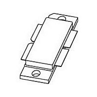
BLF369,112 NXP Semiconductors, BLF369,112 Datasheet - Page 4

BLF369,112
Manufacturer Part Number
BLF369,112
Description
RF MOSFET Small Signal RF LDMOS 65V 100A
Manufacturer
NXP Semiconductors
Datasheet
1.BLF369112.pdf
(17 pages)
Specifications of BLF369,112
Configuration
Dual Dual Source
Drain-source Breakdown Voltage
65 V
Gate-source Breakdown Voltage
13 V
Maximum Operating Temperature
+ 200 C
Minimum Operating Temperature
- 65 C
Mounting Style
Screw
Resistance Drain-source Rds (on)
0.04 Ohm (Typ) @ 14.5 V
Transistor Polarity
N-Channel
Package / Case
LDMOST
Application
HF/VHF/UHF
Channel Type
N
Channel Mode
Enhancement
Drain Source Voltage (max)
65V
Output Power (max)
500W
Power Gain (typ)@vds
18@32V/19@32V/19@32VdB
Frequency (max)
500MHz
Package Type
LDMOST
Pin Count
5
Forward Transconductance (typ)
15S
Drain Source Resistance (max)
40(Typ)@14.5Vmohm
Input Capacitance (typ)@vds
400@32VpF
Output Capacitance (typ)@vds
230@32VpF
Reverse Capacitance (typ)
15@32VpF
Operating Temp Range
-65C to 200C
Drain Efficiency (typ)
60%
Mounting
Screw
Mode Of Operation
2-Tone Class-AB/CW Class-AB/Pulsed RF Class-AB
Number Of Elements
2
Vswr (max)
10
Screening Level
Military
Lead Free Status / RoHS Status
Lead free / RoHS Compliant
Other names
934059725112 BLF369
NXP Semiconductors
6. Characteristics
Table 6.
T
[1]
[2]
BLF369_4
Product data sheet
Symbol
V
V
I
I
I
g
R
C
C
C
DSS
DSX
GSS
j
fs
(BR)DSS
GS(th)
DS(on)
iss
oss
rss
= 25 C unless otherwise specified.
I
C
D
iss
is the drain current.
and C
Characteristics
Parameter
drain-source breakdown voltage
gate-source threshold voltage
drain leakage current
drain cut-off current
gate leakage current
forward transconductance
drain-source on-state resistance
input capacitance
output capacitance
reverse transfer capacitance
oss
include reverse transfer capacitance (C
Fig 2.
V
Output capacitance as a function of drain-source voltage; typical values per
section
GS
= 0 V; f = 1 MHz.
C
Rev. 04 — 19 February 2009
(pF)
Conditions
V
V
V
V
V
V
V
V
V
V
oss
600
400
200
GS
DS
GS
GS
GS
GS
GS
GS
GS
GS
rss
0
).
= 20 V; I
0
= 0 V; I
= 0 V; V
= V
= 20 V; V
= 20 V; I
= V
= 0 V; V
= 0 V; V
= 0 V; V
GS(th)
GS(th)
D
10
DS
DS
DS
DS
D
D
= 6 mA
+ 9 V; V
+ 9 V; I
DS
= 600 mA
= 13 A
= 32 V
= 32 V; f = 1 MHz
= 32 V; f = 1 MHz
= 32 V; f = 1 MHz
= 0 V
20
D
DS
= 13 A
= 10 V
Multi-use VHF power LDMOS transistor
30
[1]
[1]
[1]
[1]
[2]
[2]
40
001aae484
V
DS
Min
65
4
-
-
-
-
-
-
-
-
(V)
50
Typ
-
-
-
100
-
15
40
400
230
15
© NXP B.V. 2009. All rights reserved.
BLF369
Max
-
5.5
4.2
-
60
-
-
-
-
-
Unit
V
V
A
nA
S
m
pF
pF
pF
4 of 17
A


