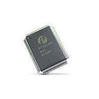
PI7C21P100BNHE Pericom Semiconductor, PI7C21P100BNHE Datasheet - Page 15

PI7C21P100BNHE
Manufacturer Part Number
PI7C21P100BNHE
Description
Peripheral Drivers & Components (PCIs) PCI-X to PCI-XBridge 2 Port
Manufacturer
Pericom Semiconductor
Datasheet
1.PI7C21P100BNHE.pdf
(79 pages)
Specifications of PI7C21P100BNHE
Maximum Operating Temperature
+ 70 C
Minimum Operating Temperature
0 C
Mounting Style
SMD/SMT
Operating Supply Voltage
3 V to 3.6 V
Package / Case
CSBGA-304
Lead Free Status / RoHS Status
Lead free / RoHS Compliant
Available stocks
Company
Part Number
Manufacturer
Quantity
Price
Company:
Part Number:
PI7C21P100BNHE
Manufacturer:
Pericom
Quantity:
135
Company:
Part Number:
PI7C21P100BNHE
Manufacturer:
PI
Quantity:
1 831
3.2.5
CLOCK SIGNALS
Name
S_CBE[7:4]#
S_PAR64
S_REQ64#
S_ACK64#
Name
P_CLK
S_CLK
Pin #
Y10, AB10, AA11,
AC8
AA10
AB13
AA8
Pin #
E21
AB23
Page 15 of 79
Type
Type
STS
STS
TS
TS
I
I
Description
Secondary Upper 32-bit Command/Byte Enables:
Multiplexed command field and byte enable field.
During address phase, the initiator drives the transaction
type on these pins. The initiator then drives the byte
enables during data phases. During bus idle,
PI7C21P100B drives S_CBE[7:0] to a valid logic level
when the bridge is granted the bus.
Secondary Upper 32-bit Parity: S_PAR64 carries the
even parity of S_AD[63:32] and S_CBE[7:4] for both
address and data phases. S_PAR64 is driven by the
initiator and is valid 1 cycle after the first address phase
when a dual address command is used and S_REQ64# is
asserted. S_PAR64 is valid 1 clock cycle after the
second address phase of a dual address transaction when
S_REQ64# is asserted. S_PAR64 is valid 1 cycle after
valid data is driven when both S_REQ64# and
S_ACK64# are asserted for that data phase. S_PAR64 is
driven by the device driving read or write data 1 cycle
after the S_AD lines are driven. S_PAR64 is tri-stated 1
cycle after the S_AD lines are tri-stated. Devices receive
data sample S_PAR64 as an input to check for possible
parity errors during 64-bit transactions. When not driven,
S_PAR64 is pulled up to a valid logic level through
external resistors.
Secondary 64-bit Transfer Request: S_REQ64# is
asserted by the initiator to indicate that the initiator is
requesting a 64-bit data transfer. S_REQ64# has the
same timing as S_FRAME#. When S_REQ64# is
asserted LOW during reset, a 64-bit data path is
supported. When S_REQ64# is HIGH during reset,
PI7C21P100B drives S_AD[63:32], S_CBE[7:4], and
S_PAR64 to valid logic levels. When deasserting,
S_REQ64# is driven to a deasserted state for 1 cycle and
then sustained by an external pull-up resistor.
Secondary 64-bit Transfer Acknowledge: S_ACK64#
is asserted by the target only when S_REQ64# is
asserted by the initiator to indicate the target’s ability to
transfer data using 64 bits. S_ACK64# has the same
timing as S_DEVSEL#. When deasserting, S_ACK64#
is driven to a deasserted state for 1 cycle and then is
sustained by an external pull-up resistor.
Description
Primary Clock Input: Provides timing for all
transactions on the primary interface. For conventional
PCI mode, the input clock frequency may be between 0
– 66MHz. In PCI-X mode, the input clock frequency
may be between 66 – 133MHz. See Section 6 for
limitations.
Secondary Clock Input: Provides timing for all
transactions on the secondary interface. For conventional
PCI mode, the input clock frequency may be between 0
– 66MHz. In PCI-X mode, the input clock frequency
may be between 66 – 133MHz. See Section 6 for
limitations. If the primary bus is running at 133MHz,
the minimum frequency that may be supplied to S_CLK
is 33MHz.
2-PORT PCI-X TO PCI-X BRIDGE
November 2005 – Revision 1.02
PI7C21P100B


