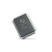
PI7C21P100BNHE Pericom Semiconductor, PI7C21P100BNHE Datasheet - Page 64

PI7C21P100BNHE
Manufacturer Part Number
PI7C21P100BNHE
Description
Peripheral Drivers & Components (PCIs) PCI-X to PCI-XBridge 2 Port
Manufacturer
Pericom Semiconductor
Datasheet
1.PI7C21P100BNHE.pdf
(79 pages)
Specifications of PI7C21P100BNHE
Maximum Operating Temperature
+ 70 C
Minimum Operating Temperature
0 C
Mounting Style
SMD/SMT
Operating Supply Voltage
3 V to 3.6 V
Package / Case
CSBGA-304
Lead Free Status / RoHS Status
Lead free / RoHS Compliant
Available stocks
Company
Part Number
Manufacturer
Quantity
Price
Company:
Part Number:
PI7C21P100BNHE
Manufacturer:
Pericom
Quantity:
135
Company:
Part Number:
PI7C21P100BNHE
Manufacturer:
PI
Quantity:
1 831
8.1.62
8.1.63
PCI-TO-PCI BRIDGE SUPPORT EXTENSION REGISTER – OFFSET
94h
SECONDARY BUS PRIVATE DEVICE MASK REGISTER – OFFSET
B0h
BIT
14:13
12:9
8
7:2
1:0
BIT
31:24
23
22
21:16
BIT
31:30
29
28:26
25
24
23
FUNCTION
Data Scale
Data Select
PME Enable
RESERVED
Power State
FUNCTION
Data Register
Bus Power / Clock
Control
B2/B3 Support for
D3
RESERVED
FUNCTION
RESERVED
Private Device Mask 13
RESERVED
Private Device Mask 9
RESERVED
Private Device Mask 7
HOT
TYPE
TYPE
RO
RO
TYPE
RW
RW
RW
RO
RO
RO
RO
RW
RO
RO
RW
RW
RW
Page 64 of 79
DESCRIPTION
Data Scale
Returns 00 when read indicating the data register is not implemented.
Data Select
Returns 0000 when read indicating the data register is not
implemented.
PME Enable
Returns 0 when read indication PME# generation is not supported.
Reserved. Returns 000000 when read.
Power State
Determines and reflects the current power state. If an un-
implemented power state is written to this register, the bridge
completes the write transaction, ignores the write data, and does not
change the value of this field. Writing a value of D0 when the
previous state was D3 will cause a device reset to occur without
activating the secondary S_RST#.
00
01
10
11
Reset to 00
DESCRIPTION
Data Register
Returns 0 when read indicating the data register is not implemented.
Bus Power / Clock Control
Returns 0 when read indicating the bus power / clock control is
disabled and the secondary clock cannot be controlled by
PI7C21P100B.
B2/B3 Support for D3
Returns 0 when read indicating B2/B3 support for D3
management state is disabled.
Reserved. Returns 000000 when read.
DESCRIPTION
Reserved. Returns 00 when read.
Private Device Mast 13
0: Rerouting disabled for device 13
1: Block assertion of S_AD[29] for configuration transactions to
device 13 and assert S_AD[31] instead.
Reserved. Returns 000 when read.
Private Device Mask 9
0: Rerouting disabled for device 9
1: Block assertion of S_AD[25] for configuration transactions to
device 9 and assert S_AD[31] instead.
Reserved. Returns 0 when read.
Private Device Mask 7
0: Rerouting disabled for device 7
1: Block assertion of S_AD[23] for configuration transactions to
device 7 and assert S_AD[31] instead.
D0
D1 (not supported)
D2 (not supported)
D3
2-PORT PCI-X TO PCI-X BRIDGE
HOT
November 2005 – Revision 1.02
PI7C21P100B
HOT
power


