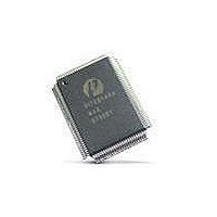
PI7C21P100BNHE Pericom Semiconductor, PI7C21P100BNHE Datasheet - Page 66

PI7C21P100BNHE
Manufacturer Part Number
PI7C21P100BNHE
Description
Peripheral Drivers & Components (PCIs) PCI-X to PCI-XBridge 2 Port
Manufacturer
Pericom Semiconductor
Datasheet
1.PI7C21P100BNHE.pdf
(79 pages)
Specifications of PI7C21P100BNHE
Maximum Operating Temperature
+ 70 C
Minimum Operating Temperature
0 C
Mounting Style
SMD/SMT
Operating Supply Voltage
3 V to 3.6 V
Package / Case
CSBGA-304
Lead Free Status / RoHS Status
Lead free / RoHS Compliant
Available stocks
Company
Part Number
Manufacturer
Quantity
Price
Company:
Part Number:
PI7C21P100BNHE
Manufacturer:
Pericom
Quantity:
135
Company:
Part Number:
PI7C21P100BNHE
Manufacturer:
PI
Quantity:
1 831
9
9.1
9.2
9.3
IEEE 1149.1 COMPATIBLE JTAG CONTROLLER
An IEEE 1149.1 compatible Test Access Port (TAP) controller and associated TAP pins are
provided to support boundary scan in PI721P100 for board-level continuity test and
diagnostics. The TAP pins assigned are TCK, TDI, TDO, TMS and TRST#. All digital input,
output, input/output pins are tested except TAP pins.
The IEEE 1149.1 Test Logic consists of a TAP controller, an instruction register, and
a group of test data registers including Bypass and Boundary Scan registers. The TAP
controller is a synchronous 16-state machine driven by the Test Clock (TCK) and the Test
Mode Select (TMS) pins. An independent power on reset circuit is provided to ensure the
machine is in TEST_LOGIC_RESET state at power-up. The JTAG signal lines are not active
when the PCI resource is operating PCI bus cycles.
INSTRUCTION REGISTER
PI7C21P100B implements a 4-bit Instruction register to control the operation of the JTAG
logic. The defined instruction codes are shown in. Those bit combinations that are not listed
are equivalent to the BYPASS (1111) instruction:
BYPASS REGISTER
The required bypass register, a one-bit shift register, provides the shortest path between TDI
and TDO when a bypass instruction is in effect. This allows rapid movement of test data to
and from other components on the board. This path can be selected when no test operation is
being performed on the PI7C21P100B.
DEVICE ID REGISTER
This register identifies Pericom as the manufacturer of the device and details the part number
and revision number for the device.
Instruction
EXTEST
SAMPLE
HIGHZ
IDCODE
BYPASS
INT_SCAN
BIT
31:28
27:12
11:0
Operation Code (binary)
TYPE
RO
RO
RO
0000
0100
0101
0110
1111
0010
VALUE
01A7h
47Fh
0h
Page 66 of 79
Bypass
Device ID
Internal Scan
Register Selected
Boundary Scan
Boundary Scan
Bypass
DESCRIPTION
Version number
Last 4 digits (hex) of the die part number
Pericom identifier assigned by JEDEC
Bit 0 is set to 1
2-PORT PCI-X TO PCI-X BRIDGE
Operation
Drives / receives off-chip test data
Samples inputs / pre-loads outputs
Tri-states outputs
Accesses the Device ID register, to read
manufacturer ID, part number, and version
number
Selected Bypass Register
Scan test
November 2005 – Revision 1.02
PI7C21P100B


