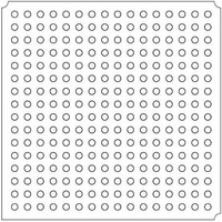
LFXP2-8E-5FTN256I Lattice, LFXP2-8E-5FTN256I Datasheet - Page 111

LFXP2-8E-5FTN256I
Manufacturer Part Number
LFXP2-8E-5FTN256I
Description
FPGA - Field Programmable Gate Array 8K LUTs 201 I/O Inst on DSP 1.2V -5 Spd
Manufacturer
Lattice
Datasheet
1.LFXP2-8E-5FTN256I.pdf
(341 pages)
Specifications of LFXP2-8E-5FTN256I
Number Of Macrocells
8000
Number Of Programmable I/os
201
Data Ram Size
226304
Supply Voltage (max)
1.26 V
Maximum Operating Temperature
+ 100 C
Minimum Operating Temperature
- 40 C
Mounting Style
SMD/SMT
Supply Voltage (min)
1.14 V
Package / Case
FTBGA-256
Number Of Logic Elements/cells
*
Number Of Labs/clbs
*
Total Ram Bits
226304
Number Of I /o
201
Number Of Gates
-
Voltage - Supply
1.14 V ~ 1.26 V
Mounting Type
*
Operating Temperature
-40°C ~ 100°C
Package
256FTBGA
Family Name
LatticeXP2
Device Logic Units
8000
Typical Operating Supply Voltage
1.2 V
Maximum Number Of User I/os
201
Ram Bits
226304
Re-programmability Support
Yes
Lead Free Status / RoHS Status
Lead free / RoHS Compliant
Available stocks
Company
Part Number
Manufacturer
Quantity
Price
Company:
Part Number:
LFXP2-8E-5FTN256I
Manufacturer:
Lattice Semiconductor Corporation
Quantity:
10 000
- Current page: 111 of 341
- Download datasheet (10Mb)
Lattice Semiconductor
chronous DRAM and synchronous SRAM devices respectively). This capability is also used in conjunction with off-
chip resistors to emulate LVPECL, and BLVDS output drivers.
Table 8-7. Programmable Drive Values for Differential Buffers
PCI Support with Programmable PCICLAMP
Each sysIO buffer can be configured to support PCI33. The buffers on the top and bottom sides of the device have
an optional PCI clamp diode that may optionally be specified in the ispLEVER design tools.
Programmable PCICLAMP can be turned ON or OFF. This option is available on each I/O independently on the top
and bottom side banks.
Programmable Input Delay
Each input can optionally be delayed before it is passed to the core logic or input registers. The primary use for the
input delay is to achieve zero hold time for the input registers when using a direct drive primary clock. To arrive at
zero hold time, the input delay will delay the data by at least as much as the primary clock injection delay. This
option can be turned ON or OFF for each I/O independently in the software using the FIXEDDELAY attribute. This
attribute is described in more detail in the software sysIO attribute section. Appendix A shows how this feature can
be enabled in the software using HDL attributes.
Software sysIO Attributes
sysIO attributes can be specified in the HDL, using the Spreadsheet view of the Design Planner or in the ASCII
preference file (.lpf) file directly. Appendices A, B and C list examples of how these can be assigned using each of
these methods. This section describes each of these attributes in detail.
IO_TYPE
This is used to set the sysIO standard for an I/O. The V
the attribute names itself. There is no separate attribute to set the V
I/O types.
HSTL15D_I
HSTL18D_I
SSTL25D_I
SSTL25D_II
SSTL18D_II
Differential I/O Standard
8-7
CCIO
Programmable Drive (mA)
required to set these I/O standards are embedded in
CCIO
16, 20
8, 12
8, 12
8, 12
4, 8
requirements. Table 8-8 lists the available
LatticeXP2 sysIO Usage Guide
Related parts for LFXP2-8E-5FTN256I
Image
Part Number
Description
Manufacturer
Datasheet
Request
R

Part Number:
Description:
FPGA - Field Programmable Gate Array 8K LUTs 100I/O Inst- on DSP 1.2V -5 Spd
Manufacturer:
Lattice
Datasheet:

Part Number:
Description:
FPGA - Field Programmable Gate Array 8K LUTs 201I/O Inst- on DSP 1.2V -5 Spd
Manufacturer:
Lattice
Datasheet:

Part Number:
Description:
FPGA - Field Programmable Gate Array 8K LUTs 100 I/O Inst on DSP 1.2V -5 Spd
Manufacturer:
Lattice
Datasheet:

Part Number:
Description:
IC, LATTICEXP2 FPGA, 435MHZ, QFP-208
Manufacturer:
LATTICE SEMICONDUCTOR
Datasheet:

Part Number:
Description:
FPGA - Field Programmable Gate Array 8K LUTs 86I/O Inst- on DSP 1.2V -5 Spd
Manufacturer:
Lattice

Part Number:
Description:
FPGA - Field Programmable Gate Array 8K LUTs 201I/O Inst- on DSP 1.2V -7 Spd
Manufacturer:
Lattice
Datasheet:
Part Number:
Description:
FPGA LatticeXP2 Family 8000 Cells Flash Technology 1.2V 144-Pin TQFP
Manufacturer:
LATTICE SEMICONDUCTOR
Datasheet:

Part Number:
Description:
IC DSP 8KLUTS 146I/O 208PQFP
Manufacturer:
Lattice
Datasheet:

Part Number:
Description:
IC DSP 8KLUTS 100I/O 144TQFP
Manufacturer:
Lattice
Datasheet:

Part Number:
Description:
IC DSP 8KLUTS 86I/O 132CSBGA
Manufacturer:
Lattice
Datasheet:

Part Number:
Description:
IC DSP 8KLUTS 86I/O 132CSBGA
Manufacturer:
Lattice
Datasheet:

Part Number:
Description:
IC DSP 8KLUTS 146I/O 208PQFP
Manufacturer:
Lattice
Datasheet:

Part Number:
Description:
IC DSP 8KLUTS 201I/O 256FTBGA
Manufacturer:
Lattice
Datasheet:

Part Number:
Description:
IC FPGA 8KLUTS 86I/O 132-BGA
Manufacturer:
Lattice
Datasheet:

Part Number:
Description:
IC FPGA 8KLUTS 86I/O 132-BGA
Manufacturer:
Lattice
Datasheet:


