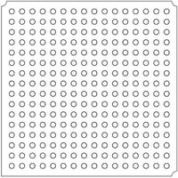
LFXP2-8E-5FTN256I Lattice, LFXP2-8E-5FTN256I Datasheet - Page 310

LFXP2-8E-5FTN256I
Manufacturer Part Number
LFXP2-8E-5FTN256I
Description
FPGA - Field Programmable Gate Array 8K LUTs 201 I/O Inst on DSP 1.2V -5 Spd
Manufacturer
Lattice
Datasheet
1.LFXP2-8E-5FTN256I.pdf
(341 pages)
Specifications of LFXP2-8E-5FTN256I
Number Of Macrocells
8000
Number Of Programmable I/os
201
Data Ram Size
226304
Supply Voltage (max)
1.26 V
Maximum Operating Temperature
+ 100 C
Minimum Operating Temperature
- 40 C
Mounting Style
SMD/SMT
Supply Voltage (min)
1.14 V
Package / Case
FTBGA-256
Number Of Logic Elements/cells
*
Number Of Labs/clbs
*
Total Ram Bits
226304
Number Of I /o
201
Number Of Gates
-
Voltage - Supply
1.14 V ~ 1.26 V
Mounting Type
*
Operating Temperature
-40°C ~ 100°C
Package
256FTBGA
Family Name
LatticeXP2
Device Logic Units
8000
Typical Operating Supply Voltage
1.2 V
Maximum Number Of User I/os
201
Ram Bits
226304
Re-programmability Support
Yes
Lead Free Status / RoHS Status
Lead free / RoHS Compliant
Available stocks
Company
Part Number
Manufacturer
Quantity
Price
Company:
Part Number:
LFXP2-8E-5FTN256I
Manufacturer:
Lattice Semiconductor Corporation
Quantity:
10 000
- Current page: 310 of 341
- Download datasheet (10Mb)
Lattice Semiconductor
Note that the calculated CRC is based on the particular arrangement of configuration memory for a particular
design. Consequently, the expected CRC results cannot be specified until after the design is placed and routed.
The ispLEVER
updates the 32-bit SED CRC register contents during bitstream generation.
The following sections describe the LatticeXP2 SED implementation and flow, along with some sample code to get
started with.
Basic SED and One-shot SED Modes
Basic SED
Basic SED checks the CRC for all bits. For Basic SED (SEDBA), the inputs are SEDCLKIN, SEDENABLE, SED-
START, and SEDFRCERRN. The output signals are SEDCLKOUT, SEDDONE, SEDINPROG, and SEDERR.
Once an error is detected the SEDERR signal will stay high. SED supports the following Soft Error Corrections
(SEC): “Do Nothing” or on-demand user reconfiguration by pulling the PROGAMN pin low from another device.
One-Shot SED
The One-Shot SED setting is based on the One-Shot Fuse. The module (SEDBB) has no input ports. The output
signals are SEDDONE, SEDINPROG, and SEDERR. At a minimum, the user must connect SEDERR to an I/O pin
in order to detect an error.
Hardware Description
As shown in Figure 16-2, the LatticeXP2 SED hardware has several inputs and outputs that allow the user to con-
trol, and monitor, SED behavior.
Figure 16-2. Signal Block Diagram
Signal Descriptions
Table 16-1. SED Signal Descriptions
®
bitstream generation software analyzes the configuration of a placed and routed design and
SEDCLKIN
SEDENABLE
SEDCLKOUT
SEDSTART
SEDINPROG
SEDDONE
SEDFRCERRN
SEDERR
Signal Name
SEDENABLE
SEDSTART
SEDFRCERRN
SEDCLKIN
(From Internal
Oscillator)
Direction
Output
Output
Output
Output
Input
Input
Input
Input
Hardware
Block
16-2
SED
Active
High
High
High
High
High
Low
N/A
N/A
SEDCLKOUT
SEDDONE
SEDINPROG
SEDERR
Clock
SED enable
Output clock
Start SED cycle
SED cycle is in progress
SED cycle is complete
Force an SED error flag
SED error flag
Description
Detection Usage Guide
LatticeXP2 Soft Error
Related parts for LFXP2-8E-5FTN256I
Image
Part Number
Description
Manufacturer
Datasheet
Request
R

Part Number:
Description:
FPGA - Field Programmable Gate Array 8K LUTs 100I/O Inst- on DSP 1.2V -5 Spd
Manufacturer:
Lattice
Datasheet:

Part Number:
Description:
FPGA - Field Programmable Gate Array 8K LUTs 201I/O Inst- on DSP 1.2V -5 Spd
Manufacturer:
Lattice
Datasheet:

Part Number:
Description:
FPGA - Field Programmable Gate Array 8K LUTs 100 I/O Inst on DSP 1.2V -5 Spd
Manufacturer:
Lattice
Datasheet:

Part Number:
Description:
IC, LATTICEXP2 FPGA, 435MHZ, QFP-208
Manufacturer:
LATTICE SEMICONDUCTOR
Datasheet:

Part Number:
Description:
FPGA - Field Programmable Gate Array 8K LUTs 86I/O Inst- on DSP 1.2V -5 Spd
Manufacturer:
Lattice

Part Number:
Description:
FPGA - Field Programmable Gate Array 8K LUTs 201I/O Inst- on DSP 1.2V -7 Spd
Manufacturer:
Lattice
Datasheet:
Part Number:
Description:
FPGA LatticeXP2 Family 8000 Cells Flash Technology 1.2V 144-Pin TQFP
Manufacturer:
LATTICE SEMICONDUCTOR
Datasheet:

Part Number:
Description:
IC DSP 8KLUTS 146I/O 208PQFP
Manufacturer:
Lattice
Datasheet:

Part Number:
Description:
IC DSP 8KLUTS 100I/O 144TQFP
Manufacturer:
Lattice
Datasheet:

Part Number:
Description:
IC DSP 8KLUTS 86I/O 132CSBGA
Manufacturer:
Lattice
Datasheet:

Part Number:
Description:
IC DSP 8KLUTS 86I/O 132CSBGA
Manufacturer:
Lattice
Datasheet:

Part Number:
Description:
IC DSP 8KLUTS 146I/O 208PQFP
Manufacturer:
Lattice
Datasheet:

Part Number:
Description:
IC DSP 8KLUTS 201I/O 256FTBGA
Manufacturer:
Lattice
Datasheet:

Part Number:
Description:
IC FPGA 8KLUTS 86I/O 132-BGA
Manufacturer:
Lattice
Datasheet:

Part Number:
Description:
IC FPGA 8KLUTS 86I/O 132-BGA
Manufacturer:
Lattice
Datasheet:


