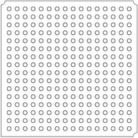
LFXP2-8E-5FTN256I Lattice, LFXP2-8E-5FTN256I Datasheet - Page 221

LFXP2-8E-5FTN256I
Manufacturer Part Number
LFXP2-8E-5FTN256I
Description
FPGA - Field Programmable Gate Array 8K LUTs 201 I/O Inst on DSP 1.2V -5 Spd
Manufacturer
Lattice
Datasheet
1.LFXP2-8E-5FTN256I.pdf
(341 pages)
Specifications of LFXP2-8E-5FTN256I
Number Of Macrocells
8000
Number Of Programmable I/os
201
Data Ram Size
226304
Supply Voltage (max)
1.26 V
Maximum Operating Temperature
+ 100 C
Minimum Operating Temperature
- 40 C
Mounting Style
SMD/SMT
Supply Voltage (min)
1.14 V
Package / Case
FTBGA-256
Number Of Logic Elements/cells
*
Number Of Labs/clbs
*
Total Ram Bits
226304
Number Of I /o
201
Number Of Gates
-
Voltage - Supply
1.14 V ~ 1.26 V
Mounting Type
*
Operating Temperature
-40°C ~ 100°C
Package
256FTBGA
Family Name
LatticeXP2
Device Logic Units
8000
Typical Operating Supply Voltage
1.2 V
Maximum Number Of User I/os
201
Ram Bits
226304
Re-programmability Support
Yes
Lead Free Status / RoHS Status
Lead free / RoHS Compliant
Available stocks
Company
Part Number
Manufacturer
Quantity
Price
Company:
Part Number:
LFXP2-8E-5FTN256I
Manufacturer:
Lattice Semiconductor Corporation
Quantity:
10 000
- Current page: 221 of 341
- Download datasheet (10Mb)
Lattice Semiconductor
Figure 11-21. READ Data Transfer When Using IDDRMX1A
Notes:
1. DDR memory sends DQ aligned to DQS Strobe.
2. The DQS Strobe is delayed by 90 degrees using the dedicated DQS logic.
3. DQ is now center aligned to DQS Strobe.
4. PRMBDET is the Preamble detect signal generated using the DQSBUFB primitive. This is used to generate the DDRCLKPOL signal.
5. The first set of I/O registers, A and B, capture data on the positive and negative edges of DQS.
6. I/O Register C transfers data so that both data are now aligned to negative edge of DQS.
7. DDCLKPOL signal generated will determine if the FPGA CLK going into the synchronization registers need to be inverted. The DDRCLK-
8. The I/O synchronization registers capture data on either the rising or falling edge of the FPGA clock.
9. The DATAVALID signal goes HIGH when valid data enters the FPGA core. Once DATA VALID is asserted, it stays high until the next READ
POL=0 when the FPGA CLK is LOW at the first rising edge of PRMBDET. The clock to the synchronization registers is not inverted. The
DDRCLKPOL=1 when the FPGA CLK is HIGH at the first rising edge of PRMBDET. In this case the clock to the synchronization register is
inverted.
pulse.
DDRCLKPOL= 0
DDRCLKPOL=1
IO REGISTERS
IO REGISTERS
CLK TO SYNC
CLK TO SYNC
DATAVALID
DQS at PIN
DQS at IOL
FPGA CLK
FPGA CLK
PRMBDET
DQ at PIN
DQ at IOL
QA
QB
QA
QB
A
B
C
11-17
P0
P0
N0
N0
P0
N1
P1
N0
P0
LatticeXP2 High-Speed I/O Interface
P1
P1
N1
P0
N0
P0
N0
N1
P1
Related parts for LFXP2-8E-5FTN256I
Image
Part Number
Description
Manufacturer
Datasheet
Request
R

Part Number:
Description:
FPGA - Field Programmable Gate Array 8K LUTs 100I/O Inst- on DSP 1.2V -5 Spd
Manufacturer:
Lattice
Datasheet:

Part Number:
Description:
FPGA - Field Programmable Gate Array 8K LUTs 201I/O Inst- on DSP 1.2V -5 Spd
Manufacturer:
Lattice
Datasheet:

Part Number:
Description:
FPGA - Field Programmable Gate Array 8K LUTs 100 I/O Inst on DSP 1.2V -5 Spd
Manufacturer:
Lattice
Datasheet:

Part Number:
Description:
IC, LATTICEXP2 FPGA, 435MHZ, QFP-208
Manufacturer:
LATTICE SEMICONDUCTOR
Datasheet:

Part Number:
Description:
FPGA - Field Programmable Gate Array 8K LUTs 86I/O Inst- on DSP 1.2V -5 Spd
Manufacturer:
Lattice

Part Number:
Description:
FPGA - Field Programmable Gate Array 8K LUTs 201I/O Inst- on DSP 1.2V -7 Spd
Manufacturer:
Lattice
Datasheet:
Part Number:
Description:
FPGA LatticeXP2 Family 8000 Cells Flash Technology 1.2V 144-Pin TQFP
Manufacturer:
LATTICE SEMICONDUCTOR
Datasheet:

Part Number:
Description:
IC DSP 8KLUTS 146I/O 208PQFP
Manufacturer:
Lattice
Datasheet:

Part Number:
Description:
IC DSP 8KLUTS 100I/O 144TQFP
Manufacturer:
Lattice
Datasheet:

Part Number:
Description:
IC DSP 8KLUTS 86I/O 132CSBGA
Manufacturer:
Lattice
Datasheet:

Part Number:
Description:
IC DSP 8KLUTS 86I/O 132CSBGA
Manufacturer:
Lattice
Datasheet:

Part Number:
Description:
IC DSP 8KLUTS 146I/O 208PQFP
Manufacturer:
Lattice
Datasheet:

Part Number:
Description:
IC DSP 8KLUTS 201I/O 256FTBGA
Manufacturer:
Lattice
Datasheet:

Part Number:
Description:
IC FPGA 8KLUTS 86I/O 132-BGA
Manufacturer:
Lattice
Datasheet:

Part Number:
Description:
IC FPGA 8KLUTS 86I/O 132-BGA
Manufacturer:
Lattice
Datasheet:


