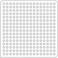
LFXP2-8E-5FTN256I Lattice, LFXP2-8E-5FTN256I Datasheet - Page 197

LFXP2-8E-5FTN256I
Manufacturer Part Number
LFXP2-8E-5FTN256I
Description
FPGA - Field Programmable Gate Array 8K LUTs 201 I/O Inst on DSP 1.2V -5 Spd
Manufacturer
Lattice
Datasheet
1.LFXP2-8E-5FTN256I.pdf
(341 pages)
Specifications of LFXP2-8E-5FTN256I
Number Of Macrocells
8000
Number Of Programmable I/os
201
Data Ram Size
226304
Supply Voltage (max)
1.26 V
Maximum Operating Temperature
+ 100 C
Minimum Operating Temperature
- 40 C
Mounting Style
SMD/SMT
Supply Voltage (min)
1.14 V
Package / Case
FTBGA-256
Number Of Logic Elements/cells
*
Number Of Labs/clbs
*
Total Ram Bits
226304
Number Of I /o
201
Number Of Gates
-
Voltage - Supply
1.14 V ~ 1.26 V
Mounting Type
*
Operating Temperature
-40°C ~ 100°C
Package
256FTBGA
Family Name
LatticeXP2
Device Logic Units
8000
Typical Operating Supply Voltage
1.2 V
Maximum Number Of User I/os
201
Ram Bits
226304
Re-programmability Support
Yes
Lead Free Status / RoHS Status
Lead free / RoHS Compliant
Available stocks
Company
Part Number
Manufacturer
Quantity
Price
Company:
Part Number:
LFXP2-8E-5FTN256I
Manufacturer:
Lattice Semiconductor Corporation
Quantity:
10 000
- Current page: 197 of 341
- Download datasheet (10Mb)
Lattice Semiconductor
The SO pin stays in the HIGHZ state throughout this command.
Figure 10-54. Bit Shifting Order
When the data buffer has filled up to one page of data, driving the Chip Select pin to high terminates the data shift-
ing. After the Chip Select pin is driven from low to high, a minimum of three clocks are required to initiate the pro-
gramming action. In the programming action, the data buffer content is copied in parallel from the data buffer into
the TAG memory Flash cells. The status bit is set to 0 when the programming actions begin. The status bit is set to
1 when the programming action is done successfully.
Figure 10-55. Data Buffer to Flash Cell Mapping
When the programming action complete, the STATUS bit is set to 1. The exact same image is written into the Flash
cells of the TAG Memory block when the programming action complete.
Figure 10-56. PROGRAM_TAG Waveform
READ_TAG (4Eh)
The READ_TAG command enables the Flash programming engine to transfer data programmed in the Flash cells
to the data buffer. The transfer action starts on the third dummy clock after the 8-bit opcode. The delay time derived
from the 21 dummy clocks is the time required to transfer the Flash cells data into the data buffer. The transfer
action, once initiated, does not need the clock to continue to run. The clock count is only required to enable the SO
pin. If the Flash circuitry is not yet enabled, the device will need extra delay time to enable the Flash circuitry before
transfer can take place. This extra delay must be provided after the third dummy clock and before the 24th dummy
clock.
If the READ_TAG command is preceded by the WRITE _EN command, then it is fast read. The device does not
require extra delay to enable the Flash circuitry.
The 20 dummy clocks after the transfer is initiated to before enabling the SO pin are considered delay clocks.
SI
Cell N-1
Flash
CS
CLK
SI
SO
Bit N-1
Bit N-1
Three Clocks To Initiate The Program Action
Shifting Clocks
8 Command
Flash Memory Cells
Optional Extra Clocks
10-47
HIGH IMPEDANCE
LatticeXP2 Memory Usage Guide
Bit 0
Bit 0
Cell 0
Flash
SO
Related parts for LFXP2-8E-5FTN256I
Image
Part Number
Description
Manufacturer
Datasheet
Request
R

Part Number:
Description:
FPGA - Field Programmable Gate Array 8K LUTs 100I/O Inst- on DSP 1.2V -5 Spd
Manufacturer:
Lattice
Datasheet:

Part Number:
Description:
FPGA - Field Programmable Gate Array 8K LUTs 201I/O Inst- on DSP 1.2V -5 Spd
Manufacturer:
Lattice
Datasheet:

Part Number:
Description:
FPGA - Field Programmable Gate Array 8K LUTs 100 I/O Inst on DSP 1.2V -5 Spd
Manufacturer:
Lattice
Datasheet:

Part Number:
Description:
IC, LATTICEXP2 FPGA, 435MHZ, QFP-208
Manufacturer:
LATTICE SEMICONDUCTOR
Datasheet:

Part Number:
Description:
FPGA - Field Programmable Gate Array 8K LUTs 86I/O Inst- on DSP 1.2V -5 Spd
Manufacturer:
Lattice

Part Number:
Description:
FPGA - Field Programmable Gate Array 8K LUTs 201I/O Inst- on DSP 1.2V -7 Spd
Manufacturer:
Lattice
Datasheet:
Part Number:
Description:
FPGA LatticeXP2 Family 8000 Cells Flash Technology 1.2V 144-Pin TQFP
Manufacturer:
LATTICE SEMICONDUCTOR
Datasheet:

Part Number:
Description:
IC DSP 8KLUTS 146I/O 208PQFP
Manufacturer:
Lattice
Datasheet:

Part Number:
Description:
IC DSP 8KLUTS 100I/O 144TQFP
Manufacturer:
Lattice
Datasheet:

Part Number:
Description:
IC DSP 8KLUTS 86I/O 132CSBGA
Manufacturer:
Lattice
Datasheet:

Part Number:
Description:
IC DSP 8KLUTS 86I/O 132CSBGA
Manufacturer:
Lattice
Datasheet:

Part Number:
Description:
IC DSP 8KLUTS 146I/O 208PQFP
Manufacturer:
Lattice
Datasheet:

Part Number:
Description:
IC DSP 8KLUTS 201I/O 256FTBGA
Manufacturer:
Lattice
Datasheet:

Part Number:
Description:
IC FPGA 8KLUTS 86I/O 132-BGA
Manufacturer:
Lattice
Datasheet:

Part Number:
Description:
IC FPGA 8KLUTS 86I/O 132-BGA
Manufacturer:
Lattice
Datasheet:


