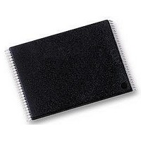
NANDO1GW3B2CN6 NUMONYX, NANDO1GW3B2CN6 Datasheet - Page 14

NANDO1GW3B2CN6
Manufacturer Part Number
NANDO1GW3B2CN6
Description
IC, FLASH, 1GB, 25µS, TSOP-48
Manufacturer
NUMONYX
Datasheet
1.NANDO1GW3B2CN6.pdf
(60 pages)
Specifications of NANDO1GW3B2CN6
Memory Type
FLASH
Memory Size
1GB
Access Time
25µS
Supply Voltage Range
2.7V TO 3.6V
Memory Case Style
TSOP
No. Of Pins
48
Operating Temperature Range
-40°C TO +85°C
Voltage, Vcc
3.3V
Memory Configuration
128M X 8
Rohs Compliant
Yes
Signals description
3
3.1
3.2
3.3
3.4
3.5
3.6
14/60
Signals description
See
connected to this device.
Inputs/outputs (I/O0-I/O7)
Input/outputs 0 to 7 are used to input the selected address, output the data during a read
operation or input a command or data during a write operation. The inputs are latched on
the rising edge of Write Enable. I/O0-I/O7 are left floating when the device is deselected or
the outputs are disabled.
Inputs/outputs (I/O8-I/O15)
Input/outputs 8 to 15 are only available in x16 devices. They are used to output the data
during a read operation or input data during a write operation. Command and address
Inputs only require I/O0 to I/O7.
The inputs are latched on the rising edge of Write Enable. I/O8-I/O15 are left floating when
the device is deselected or the outputs are disabled.
Address Latch Enable (AL)
The Address Latch Enable activates the latching of the address inputs in the command
interface. When AL is High, the inputs are latched on the rising edge of Write Enable.
Command Latch Enable (CL)
The Command Latch Enable activates the latching of the command inputs in the command
interface. When CL is High, the inputs are latched on the rising edge of Write Enable.
Chip Enable (E)
The Chip Enable input activates the memory control logic, input buffers, decoders and
sense amplifiers. When Chip Enable is Low, V
High, v
mode.
Read Enable (R)
The Read Enable pin, R, controls the sequential data output during read operations. Data is
valid t
column address counter by one.
Figure 2: Logic
RLQV
IH
, while the device is busy, the device remains selected and does not go into standby
after the falling edge of R. The falling edge of R also increments the internal
diagram, and
Table 3: Signal
IL
, the device is selected. If Chip Enable goes
names, for a brief overview of the signals
NAND01G-B2B, NAND02G-B2C


