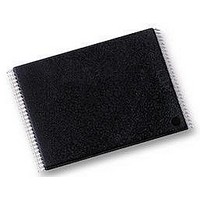
NANDO1GW3B2CN6 NUMONYX, NANDO1GW3B2CN6 Datasheet - Page 20

NANDO1GW3B2CN6
Manufacturer Part Number
NANDO1GW3B2CN6
Description
IC, FLASH, 1GB, 25µS, TSOP-48
Manufacturer
NUMONYX
Datasheet
1.NANDO1GW3B2CN6.pdf
(60 pages)
Specifications of NANDO1GW3B2CN6
Memory Type
FLASH
Memory Size
1GB
Access Time
25µS
Supply Voltage Range
2.7V TO 3.6V
Memory Case Style
TSOP
No. Of Pins
48
Operating Temperature Range
-40°C TO +85°C
Voltage, Vcc
3.3V
Memory Configuration
128M X 8
Rohs Compliant
Yes
Device operations
6
6.1
6.1.1
6.1.2
20/60
Device operations
The following section gives the details of the device operations.
Read memory array
At power-up the device defaults to read mode. To enter read mode from another mode the
Read command must be issued, see
Once a Read command is issued two types of operations are available: random read and
page read.
Random read
Each time the Read command is issued the first read is random read.
Page read
After the first random read access, the page data (2112 bytes or 1056 words) is transferred
to the page buffer in a time of t
complete the Ready/Busy signal goes High. The data can then be read out sequentially
(from selected column address to last column address) by pulsing the Read Enable signal.
The device can output random data in a page, instead of the consecutive sequential data, by
issuing a Random Data Output command.
The Random Data Output command can be used to skip some data during a sequential
data output.
The sequential operation can be resumed by changing the column address of the next data
to be output, to the address which follows the Random Data Output command.
The Random Data Output command can be issued as many times as required within a
page.
The Random Data Output command is not accepted during cache read operations.
WHBH
(refer to
Table 10:
Table 25
Commands.
for value). Once the transfer is
NAND01G-B2B, NAND02G-B2C


