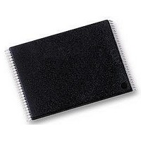
NANDO1GW3B2CN6 NUMONYX, NANDO1GW3B2CN6 Datasheet - Page 59

NANDO1GW3B2CN6
Manufacturer Part Number
NANDO1GW3B2CN6
Description
IC, FLASH, 1GB, 25µS, TSOP-48
Manufacturer
NUMONYX
Datasheet
1.NANDO1GW3B2CN6.pdf
(60 pages)
Specifications of NANDO1GW3B2CN6
Memory Type
FLASH
Memory Size
1GB
Access Time
25µS
Supply Voltage Range
2.7V TO 3.6V
Memory Case Style
TSOP
No. Of Pins
48
Operating Temperature Range
-40°C TO +85°C
Voltage, Vcc
3.3V
Memory Configuration
128M X 8
Rohs Compliant
Yes
NAND01G-B2B, NAND02G-B2C
14
Revision history
Table 30.
18-May-2006
23-Nov-2006
01-Jun-2006
09-Jun-2006
20-Apr-2007
14-Apr-2008
Date
Document revision history
Version
0.1
1
2
3
4
5
Initial release.
Document status changed to preliminary data.
VFBGA63 9 x 11 x 1 mm package added for NAND01G-B2B devices
and VFBGA63 9.5 x 12 x 1 mm dedicated to NAND02G-B2C devices.
Note 2 below
Overview of
concerning Exit Cache Read command updated in
read. Block replacement section replaced by
memory failure
t
data
RB waveform updated in
waveforms, and CL waveform modified in
waveforms.
An error correction code (ECC) is required to obtain a data integrity of
100 000 program/erase cycles per block.
Section 3.9: Ready/Busy (RB)
t
Table 25: AC characteristics for
Note removed below
t
program.
Alt. symbol for t
operations.
Applied Numonyx branding.
WHALL
RHRL2
WHBH2
input.
timing removed from
added in
replaced by t
Section 6.1: Read memory array
Commands
modes.
BLBH4
Table 24: AC characteristics for command, address,
BLBH5
Figure 11: Copy back
is t
RST
Figure 25: Page read operation AC
removed.
, cash busy time, in
Figure 9: Page program operation
in
modified.
Changes
Table 25: AC characteristics for
operations.
Figure 26: Page program AC
program.
Section 8.2: NAND flash
updated. Paragraph
Section 6.5: Cache
Section 6.2: Cache
Revision history
and
59/60


