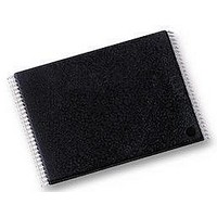
NANDO1GW3B2CN6 NUMONYX, NANDO1GW3B2CN6 Datasheet - Page 41

NANDO1GW3B2CN6
Manufacturer Part Number
NANDO1GW3B2CN6
Description
IC, FLASH, 1GB, 25µS, TSOP-48
Manufacturer
NUMONYX
Datasheet
1.NANDO1GW3B2CN6.pdf
(60 pages)
Specifications of NANDO1GW3B2CN6
Memory Type
FLASH
Memory Size
1GB
Access Time
25µS
Supply Voltage Range
2.7V TO 3.6V
Memory Case Style
TSOP
No. Of Pins
48
Operating Temperature Range
-40°C TO +85°C
Voltage, Vcc
3.3V
Memory Configuration
128M X 8
Rohs Compliant
Yes
NAND01G-B2B, NAND02G-B2C
11
DC and AC parameters
This section summarizes the operating and measurement conditions, and the DC and AC
characteristics of the device. The parameters in the DC and AC characteristics tables that
follow, are derived from tests performed under the measurement conditions summarized in
Table 20: Operating and AC measurement
operating conditions in their circuit match the measurement conditions when relying on the
quoted parameters.
Table 20.
Table 21.
1. T
2. Input/output capacitances double in stacked devices.
Supply voltage (V
Ambient temperature (T
Load capacitance (C
(1 TTL GATE and C
Input pulses voltages
Input and output timing ref. voltages
Output circuit resistor R
Input rise and fall times
Symbol
C
C
A
I/O
IN
= 25 °C, f = 1 MHz. C
Input capacitance
Input/output capacitance
Operating and AC measurement conditions
Capacitance
DD
L
)
L
)
)
A
ref
)
IN
Parameter
Parameter
and C
(1)
I/O
are not 100% tested.
(2)
3 V devices (2.7 - 3.6 V)
1.8 V devices
1.8 V devices
1.8 V devices
3 V devices
3 V devices
Grade 1
Grade 6
conditions. Designers should check that the
Test condition
V
V
IN
IL
= 0 V
= 0 V
Min
–40
1.7
2.7
0.4
0
0
NAND flash
Typ
V
DC and AC parameters
8.35
DD
30
50
5
/2
Max
1.95
V
3.6
2.4
70
85
DD
Max
10
10
Units
pF
pF
kΩ
°C
°C
Unit
ns
V
V
V
V
V
pF
pF
41/60


