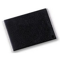
NANDO1GW3B2CN6 NUMONYX, NANDO1GW3B2CN6 Datasheet - Page 54

NANDO1GW3B2CN6
Manufacturer Part Number
NANDO1GW3B2CN6
Description
IC, FLASH, 1GB, 25µS, TSOP-48
Manufacturer
NUMONYX
Datasheet
1.NANDO1GW3B2CN6.pdf
(60 pages)
Specifications of NANDO1GW3B2CN6
Memory Type
FLASH
Memory Size
1GB
Access Time
25µS
Supply Voltage Range
2.7V TO 3.6V
Memory Case Style
TSOP
No. Of Pins
48
Operating Temperature Range
-40°C TO +85°C
Voltage, Vcc
3.3V
Memory Configuration
128M X 8
Rohs Compliant
Yes
DC and AC parameters
Figure 33. Resistor value versus waveform timings for Ready/Busy signal
1. T = 25°C.
11.2
Figure 34. Data protection
54/60
400
300
200
100
0
1
30
1.7
1.7
Data protection
The Numonyx NAND device is designed to guarantee data protection during power
transitions.
A V
In the V
low (V
figure.
DD
V DD
W
V DD = 1.8V, C L = 30pF
IL
detection circuit disables all NAND operations, if V
DD
) to guarantee hardware protection during power transitions as shown in the below
2
1.7
0.85
60
Nominal Range
range from V
R P (K
V LKO
3
Locked
0.57
1.7
90
LKO
t f
to the lower limit of nominal range, the WP pin should be kept
4
0.43
1.7
120
2
1
3
4
t r
400
300
200
100
Locked
0
1
100
3.6
2.4
ibusy
V DD = 3.3V, C L = 100pF
2
DD
NAND01G-B2B, NAND02G-B2C
200
3.6
1.2
is below the V
R P (K
Ai11086
3
300
3.6
0.8
LKO
threshold.
400
4
3.6
2
1
3
4
0.6
ai07565B


