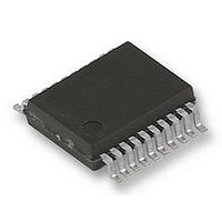
UPD78F9222MC(T)-5A4-A NEC, UPD78F9222MC(T)-5A4-A Datasheet - Page 185

UPD78F9222MC(T)-5A4-A
Manufacturer Part Number
UPD78F9222MC(T)-5A4-A
Description
8BIT MCU, 4K FLASH, 256B RAM, 78F9222
Manufacturer
NEC
Datasheet
1.UPD78F9222MCT-5A4-A.pdf
(414 pages)
Specifications of UPD78F9222MC(T)-5A4-A
Controller Family/series
UPD78
No. Of I/o's
17
Ram Memory Size
256Byte
Cpu Speed
10MHz
No. Of Timers
4
No. Of
RoHS Compliant
Core Size
8bit
Program Memory Size
4KB
Oscillator Type
External, Internal
Available stocks
Company
Part Number
Manufacturer
Quantity
Price
Company:
Part Number:
UPD78F9222MC(T)-5A4-A
Manufacturer:
NEC
Quantity:
1 000
Company:
Part Number:
UPD78F9222MC(T)-5A4-A
Manufacturer:
NEC/PBF
Quantity:
6 640
Part Number:
UPD78F9222MC(T)-5A4-A
Manufacturer:
RENESAS/瑞萨
Quantity:
20 000
- Current page: 185 of 414
- Download datasheet (4Mb)
(1) Receive buffer register 6 (RXB6)
(2) Receive shift register 6 (RXS6)
(3) Transmit buffer register 6 (TXB6)
(4) Transmit shift register 6 (TXS6)
This 8-bit register stores parallel data converted by receive shift register 6 (RXS6).
Each time 1 byte of data has been received, new receive data is transferred to this register from receive shift
register 6 (RXS6). If the data length is set to 7 bits, data is transferred as follows.
• In LSB-first reception, the receive data is transferred to bits 0 to 6 of RXB6 and the MSB of RXB6 is always 0.
• In MSB-first reception, the receive data is transferred to bits 7 to 1 of RXB6 and the LSB of RXB6 is always 0.
If an overrun error (OVE6) occurs, the receive data is not transferred to RXB6.
RXB6 can be read by an 8-bit memory manipulation instruction. No data can be written to this register.
Reset signal generation sets this register to FFH.
Caution Reception enable status is entered, after having set RXE6 to 1 and one clock of the base clock
This register converts the serial data input to the R
RXS6 cannot be directly manipulated by a program.
This buffer register is used to set transmit data. Transmission is started when data is written to TXB6.
If the data length is set to 7 bits:
This register can be read or written by an 8-bit memory manipulation instruction.
Reset signal generation sets this register to FFH.
Cautions 1. When starting transmission, write transmit data to TXB6, after having set TXE6 to 1 and a
This register transmits the data transferred from TXB6 from the T
TXB6 immediately after TXB6 is written for the first transmission, or immediately before INTST6 occurs after one
frame was transmitted for continuous transmission. Data is transferred from TXB6 and transmitted from the T
pin at the falling edge of the base clock.
TXS6 cannot be directly manipulated by a program.
• In LSB-fast transmission, data is transferred to bits 0 to 6 of TXB6, and the MSB of TXB6 is not transmitted.
• In MSB-fast transmission, data is transferred to bits 7 to 1 of TXB6, and the LSB of TXB6 is not transmitted.
(f
2. Do not write data to TXB6 when bit 1 (TXBF6) of asynchronous serial interface transmission
3. Do not refresh (write the same value to) TXB6 by software during a communication
XCLK6
wait of one clock or more of the base clock (f
status register 6 (ASIF6) is 1.
operation (when bit 7 (POWER6) and bit 6 (TXE6) of asynchronous serial interface operation
mode register 6 (ASIM6) are 1 or when bit 7 (POWER6) and bit 5 (RXE6) of ASIM6 are 1).
When outputting same values in continuous transmission, be sure to confirm that TXBF6 is
0 before writing the same values to TXB6.
) has elapsed.
CHAPTER 11 SERIAL INTERFACE UART6
User’s Manual U16898EJ5V0UD
X
D6 pin into parallel data.
XCLK6
X
D6 pin as serial data. Data is transferred from
) has been performed.
185
X
D6
Related parts for UPD78F9222MC(T)-5A4-A
Image
Part Number
Description
Manufacturer
Datasheet
Request
R

Part Number:
Description:
16/8 bit single-chip microcomputer
Manufacturer:
NEC
Datasheet:

Part Number:
Description:
Dual audio power amp circuit
Manufacturer:
NEC
Datasheet:

Part Number:
Description:
Dual comparator
Manufacturer:
NEC
Datasheet:

Part Number:
Description:
MOS type composite field effect transistor
Manufacturer:
NEC
Datasheet:

Part Number:
Description:
50 V/100 mA FET array incorporating 2 N-ch MOSFETs
Manufacturer:
NEC
Datasheet:

Part Number:
Description:
6-pin small MM high-frequency double transistor
Manufacturer:
NEC
Datasheet:

Part Number:
Description:
6-pin small MM high-frequency double transistor
Manufacturer:
NEC
Datasheet:

Part Number:
Description:
6-pin small MM high-frequency double transistor
Manufacturer:
NEC
Datasheet:

Part Number:
Description:
6-pin small MM high-frequency double transistor
Manufacturer:
NEC
Datasheet:

Part Number:
Description:
Twin transistors equipped with different model chips(6P small MM)
Manufacturer:
NEC
Datasheet:

Part Number:
Description:
Bipolar analog integrated circuit
Manufacturer:
NEC
Datasheet:


