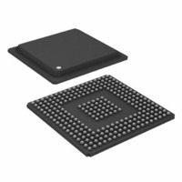
ADSP-BF535PBBZ-200 Analog Devices Inc, ADSP-BF535PBBZ-200 Datasheet - Page 10

ADSP-BF535PBBZ-200
Manufacturer Part Number
ADSP-BF535PBBZ-200
Description
200/400MMAC 16-bit DSP MICROCOMPUTER
Manufacturer
Analog Devices Inc
Series
Blackfin®r
Type
Fixed Pointr
Specifications of ADSP-BF535PBBZ-200
Interface
PCI, SPI, SSP, UART, USB
Clock Rate
200MHz
Non-volatile Memory
External
On-chip Ram
308kB
Voltage - I/o
3.30V
Voltage - Core
1.50V
Operating Temperature
-40°C ~ 85°C
Mounting Type
Surface Mount
Package / Case
260-BGA
Lead Free Status / RoHS Status
Lead free / RoHS Compliant
Available stocks
Company
Part Number
Manufacturer
Quantity
Price
Company:
Part Number:
ADSP-BF535PBBZ-200
Manufacturer:
Analog Devices Inc
Quantity:
10 000
ADSP-BF535
Serial Peripheral Interface (SPI) Ports
The ADSP-BF535 Blackfin processor has two SPI compatible
ports that enable the processor to communicate with multiple
SPI compatible devices.
The SPI interface uses three pins for transferring data: two data
pins (Master Output-Slave Input, MOSIx, and Master Input-
Slave Output, MISOx) and a clock pin (Serial Clock, SCKx).
Two SPI chip select input pins (SPISSx) let other SPI devices
select the processor, and fourteen SPI chip select output pins
(SPIxSEL7–1) let the processor select other SPI devices. The SPI
select pins are reconfigured programmable flag pins. Using these
pins, the SPI ports provide a full duplex, synchronous serial inter-
face, which supports both master and slave modes and
multimaster environments.
Each SPI port’s baud rate and clock phase/polarities are program-
mable (see
controller, configurable to support transmit or receive data
streams. The SPI’s DMA controller can only service unidirec-
tional accesses at any given time.
Framing—Each transmit and receive port can run with or
without frame sync signals for each data-word. Frame
sync signals can be generated internally or externally,
active high or low, with either of two pulse widths and
early or late frame sync.
Companding in hardware—Each SPORT can perform
A-law or µ-law companding according to ITU recommen-
dation G.711. Companding can be selected on the
transmit and/or receive channel of the SPORT without
additional latencies.
DMA operations with single-cycle overhead—Each
SPORT can automatically receive and transmit multiple
buffers of memory data. The Blackfin processor can link
or chain sequences of DMA transfers between a SPORT
and memory. The chained DMA can be dynamically
allocated and updated through the descriptor blocks that
set up the chain.
Interrupts—Each transmit and receive port generates an
interrupt upon completing the transfer of a data-word or
after transferring an entire data buffer or buffers through
the DMA.
Multichannel capability—Each SPORT supports 128
channels and is compatible with the H.100, H.110,
MVIP-90, and HMVIP standards.
Figure
Figure 4. SPI Clock Rate Calculation
SPI Clock Rate
4), and each has an integrated DMA
=
------------------------------------ -
2
SPIBAUD
f
SCLK
–10–
During transfers, the SPI ports simultaneously transmit and
receive by serially shifting data in and out on two serial data lines.
The serial clock line synchronizes the shifting and sampling of
data on the two serial data lines.
In master mode, the processor performs the following sequence
to set up and initiate SPI transfers:
1. Enables and configures the SPI port’s operation (data
2. Selects the target SPI slave with an SPIxSELy output pin
3. Defines one or more TCBs in the processor’s memory
4. Enables the SPI DMA engine and specifies transfer
5. Reads or writes the SPI port receive or transmit data
In slave mode, the processor performs the following sequence to
set up the SPI port to receive data from a master transmitter:
1. Enables and configures the SPI slave port to match the
2. Defines and generates a receive TCB in the processor’s
3. Enables the SPI DMA engine for a receive access
4. Starts receiving data on the appropriate SPI SCKx edges
In DMA mode only, reception continues until the SPI DMA
word count transitions from 1 to 0. The processor can continue,
by queuing up the next command TCB.
A slave mode transmit operation is similar, except the processor
specifies the data buffer in memory from which to transmit data,
generates and relinquishes control of the transmit TCB, and
begins filling the SPI port’s data buffer. If the SPI controller is
not ready to transmit, it can transmit a “zero” word.
UART Port
The ADSP-BF535 Blackfin processor provides two full-duplex
Universal Asynchronous Receiver/Transmitter (UART) ports
(UART0 and UART1) fully compatible with PC-standard
UARTs. The UART ports provide a simplified UART interface
to other peripherals or hosts, supporting full-duplex, DMA-sup-
ported, asynchronous transfers of serial data. Each UART port
The SCKx line generates the programmed clock pulses
for simultaneously shifting data out on MOSIx and
shifting data in on MISOx. In the DMA mode only,
transfers continue until the SPI DMA word count transi-
tions from 1 to 0.
size and transfer format).
(reconfigured programmable flag pin).
space (optional in DMA mode only).
direction (optional in DMA mode only).
buffer (in non-DMA mode only).
operation parameters set up on the master (data size and
transfer format) SPI transmitter.
memory space to interrupt at the end of the data transfer
(optional in DMA mode only).
(optional in DMA mode only).
after receiving an SPI chip select on an SPISSx input pin
(reconfigured programmable flag pin) from a master.
REV. A


