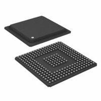
ADSP-BF535PBBZ-200 Analog Devices Inc, ADSP-BF535PBBZ-200 Datasheet - Page 13

ADSP-BF535PBBZ-200
Manufacturer Part Number
ADSP-BF535PBBZ-200
Description
200/400MMAC 16-bit DSP MICROCOMPUTER
Manufacturer
Analog Devices Inc
Series
Blackfin®r
Type
Fixed Pointr
Specifications of ADSP-BF535PBBZ-200
Interface
PCI, SPI, SSP, UART, USB
Clock Rate
200MHz
Non-volatile Memory
External
On-chip Ram
308kB
Voltage - I/o
3.30V
Voltage - Core
1.50V
Operating Temperature
-40°C ~ 85°C
Mounting Type
Surface Mount
Package / Case
260-BGA
Lead Free Status / RoHS Status
Lead free / RoHS Compliant
Available stocks
Company
Part Number
Manufacturer
Quantity
Price
Company:
Part Number:
ADSP-BF535PBBZ-200
Manufacturer:
Analog Devices Inc
Quantity:
10 000
The power dissipated by a processor is largely a function of the
clock frequency of the processor and the square of the operating
voltage. For example, reducing the clock frequency by 25%
results in a 25% reduction in power dissipation, while reducing
the voltage by 25% reduces power dissipation by more than 40%.
Further, these power savings are additive, in that if the clock
frequency and power are both reduced, the power savings are
dramatic.
Dynamic Power Management allows both the processor’s input
voltage (V
and independently controlled.
As previously explained, the savings in power dissipation can be
modeled by the following equation:
where:
As an example of how significant the power savings of Dynamic
Power Management are when both frequency and voltage are
reduced, consider an example where the frequency is reduced
from its nominal value to 50 MHz and the voltage is reduced from
its nominal value to 1.2 V. At this reduced frequency and voltage,
the processor dissipates about 10% of the power dissipated at
nominal frequency and voltage.
Peripheral Power Control
The ADSP-BF535 Blackfin processor provides additional power
control capability by allowing dynamic scheduling of clock inputs
to each of the peripherals. Clocking to each of the peripherals
listed below can be enabled or disabled by appropriately setting
the peripheral’s control bit in the peripheral clock enable register
(PLL_IOCK). The Peripheral Clock Enable Register allows indi-
vidual control for each of these peripherals:
REV. A
f
f
V
V
CCLKNOM
CCLKRED
Power Dissipation Factor
DDINTNOM
DDINTRED
PCI
EBIU controller
Programmable flags
MemDMA controller
SPORT 0
SPORT 1
SPI 0
SPI 1
UART 0
UART 1
Timer 0, Timer 1, Timer 2
USB CLK
DDINT
is the reduced core clock frequency
is the nominal core clock frequency (300 MHz)
is the reduced internal supply voltage
is the nominal internal supply voltage (1.5 V)
) and clock frequency (f
=
------------------------- -
f
f
CCLKNOM
CCLKRED
CCLK
) to be dynamically
------------------------------
V
V
DDINTNOM
DDINTRED
2
–13–
Clock Signals
The ADSP-BF535 Blackfin processor can be clocked by a sine
wave input or a buffered shaped clock derived from an external
clock oscillator.
If a buffered, shaped clock is used, this external clock connects
to the processor CLKIN pin. The CLKIN input cannot be
halted, changed, or operated below the specified frequency
during normal operation. This clock signal should be a 3.3 V
LVTTL compatible signal. The processor provides a user-pro-
grammable 1 to 31 multiplication of the input clock to
support external-to-internal clock ratios. The MSEL6–0,
BYPASS, and DF pins decide the PLL multiplication factor at
reset. At run time, the multiplication factor can be controlled in
software. The combination of pull-up and pull-down resistors in
Figure 7
produces a 150 MHz core clock from the 25 MHz input. For
other clock multiplier settings, see the ADSP-BF535 Blackfin
Processor Hardware Reference.
All on-chip peripherals operate at the rate set by the system clock
(SCLK). The system clock frequency is programmable by means
of the SSEL pins. At run time the system clock frequency can be
controlled in software by writing to the SSEL fields in the PLL
control register (PLL_CTL). The values programmed into the
RESET SOURCE
sets up a core clock ratio of 6:1, which, for example,
V
V
DD
DD
Figure 7. Clock Ratio Example
MSEL0 (PF0)
MSEL1 (PF1)
MSEL2 (PF2)
MSEL3 (PF3)
MSEL4 (PF4)
MSEL5 (PF5)
MSEL6 (PF6)
DF (PF7)
BYPASS
RESET
CLKIN
BLACKFIN PROCESSOR
ADSP-BF535
THE PULL-UP/PULL-DOWN
RESISTORS ON THE MSEL,
DF, AND BYPASS PINS SELECT
THE CORE CLOCK RATIO.
HERE, THE SELECTION (6:1)
AND 25MHz INPUT CLOCK
PRODUCE A 150MHz CORE CLOCK.
ADSP-BF535
CLKOUT


