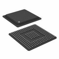
ADSP-BF535PBBZ-200 Analog Devices Inc, ADSP-BF535PBBZ-200 Datasheet - Page 19

ADSP-BF535PBBZ-200
Manufacturer Part Number
ADSP-BF535PBBZ-200
Description
200/400MMAC 16-bit DSP MICROCOMPUTER
Manufacturer
Analog Devices Inc
Series
Blackfin®r
Type
Fixed Pointr
Specifications of ADSP-BF535PBBZ-200
Interface
PCI, SPI, SSP, UART, USB
Clock Rate
200MHz
Non-volatile Memory
External
On-chip Ram
308kB
Voltage - I/o
3.30V
Voltage - Core
1.50V
Operating Temperature
-40°C ~ 85°C
Mounting Type
Surface Mount
Package / Case
260-BGA
Lead Free Status / RoHS Status
Lead free / RoHS Compliant
Available stocks
Company
Part Number
Manufacturer
Quantity
Price
Company:
Part Number:
ADSP-BF535PBBZ-200
Manufacturer:
Analog Devices Inc
Quantity:
10 000
Table 7. Pin Descriptions (continued)
REV. A
Pin
TRST
RESET
CLKIN1
BYPASS
DEEPSLEEP
BMODE2–0
PCI_AD31–0
PCI_CBE3–0
PCI_FRAME
PCI_IRDY
PCI_TRDY
PCI_DEVSEL
PCI_STOP
PCI_PERR
PCI_PAR
PCI_REQ
PCI_SERR
PCI_RST
PCI_GNT
PCI_IDSEL
PCI_LOCK
PCI_CLK
PCI_INTA
PCI_INTB
PCI_INTC
PCI_INTD
XTAL1
XTAL0
EMU
V
V
V
V
V
GND
Type column symbols: G = Ground, I = Input, O = Output, P = Power supply, T = Three-state
DDPLL
DDRTC
DDEXT
DDPCIEXT
DDINT
Type Function
I
I
I
I
O
I
I/O/T PCI address and data bus.
I/O/T PCI byte enables.
I/O/T PCI frame signal. Used by PCI initiators for signalling the beginning and end of a PCI
I/O/T PCI initiator ready signal.
I/O/T PCI target ready signal.
I/O/T PCI device select signal. Asserted by targets of PCI transactions to claim the transaction.
I/O/T PCI stop signal.
I/O/T PCI parity error signal.
I/O/T PCI parity signal.
O
I/O/T PCI system error signal. Requires a pull-up on the system board.
I/O/T PCI reset signal.
I
I
I
I
I/O/T PCI interrupt A line on PCI bus. Asserted by the ADSP-BF535 Blackfin processor as a
I
I
I
I
O
O
P
P
P
P
P
G
JTAG reset.
When this pin is asserted to logic zero level for at least 10 CLKIN cycles, a hardware reset
is initiated. The minimum pulse width for power-on reset is 40 µs.
Clock in.
Dedicated mode pin. May be permanently strapped to V
PLL.
Denotes that the Blackfin processor core is in Deep Sleep mode.
Dedicated mode pin. May be permanently strapped to V
mode that is employed following hardware reset or software reset.
transaction.
PCI request signal. Used for requesting the use of the PCI bus.
PCI grant signal. Used for granting access to the PCI bus.
PCI initialization device select signal. Individual device selects for targets of PCI config-
uration transactions.
PCI lock signal. Used to lock a target or the entire PCI bus for use by the master that
asserts the lock.
PCI clock.
device-to-signal an interrupt to the system processor. Monitored by the ADSP-BF535
when acting as the system processor.
PCI interrupt B line. Monitored by ADSP-BF535 Blackfin processor when acting as the
system processor.
PCI interrupt C line. Monitored by the ADSP-BF535 Blackfin processor when acting as
the system processor.
PCI interrupt D line. Monitored by the ADSP-BF535 Blackfin processor when acting as
the system processor.
Real-Time Clock oscillator input.
Real-Time Clock oscillator output.
Emulator acknowledge, open drain. Must be connected to the ADSP-BF535 Blackfin
processor emulator target board connector only.
PLL power supply (1.5 V nominal).
Real-Time Clock power supply (3.3 V nominal).
I/O (except PCI) power supply (3.3 V nominal).
PCI I/O power supply (3.3 V nominal).
Internal power supply (1.5 V nominal).
Power supply return.
–19–
DD
DD
or V
or V
ADSP-BF535
SS
SS
. Bypasses the on-chip
. Configures the boot


