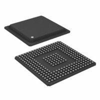
ADSP-BF535PBBZ-200 Analog Devices Inc, ADSP-BF535PBBZ-200 Datasheet - Page 18

ADSP-BF535PBBZ-200
Manufacturer Part Number
ADSP-BF535PBBZ-200
Description
200/400MMAC 16-bit DSP MICROCOMPUTER
Manufacturer
Analog Devices Inc
Series
Blackfin®r
Type
Fixed Pointr
Specifications of ADSP-BF535PBBZ-200
Interface
PCI, SPI, SSP, UART, USB
Clock Rate
200MHz
Non-volatile Memory
External
On-chip Ram
308kB
Voltage - I/o
3.30V
Voltage - Core
1.50V
Operating Temperature
-40°C ~ 85°C
Mounting Type
Surface Mount
Package / Case
260-BGA
Lead Free Status / RoHS Status
Lead free / RoHS Compliant
Available stocks
Company
Part Number
Manufacturer
Quantity
Price
Company:
Part Number:
ADSP-BF535PBBZ-200
Manufacturer:
Analog Devices Inc
Quantity:
10 000
ADSP-BF535
Table 7. Pin Descriptions (continued)
Pin
PF4/SPI0SEL2/MSEL4 I/O
PF3/SPI1SEL1/MSEL3 I/O
PF2/SPI0SEL1/MSEL2 I/O
PF1/SPISS1/MSEL1
PF0/SPISS0/MSEL0
RSCLK0
RFS0
DR0
TSCLK0
TFS0
DT0
RSCLK1
RFS1
DR1
TSCLK1
TFS1
DT1
MOSI0
MISO0
SCK0
MOSI1
MISO1
SCK1
RX0
TX0
RX1
TX1
USB_CLK
XVER_DATA
DPLS
DMNS
TXDPLS
TXDMNS
TXEN
SUSPEND
NMI
TCK
TDO
TDI
TMS
Type column symbols: G = Ground, I = Input, O = Output, P = Power supply, T = Three-state
Type Function
I/O
I/O
I/O/T Receive serial clock for SPORT0.
I/O/T Receive frame synchronization for SPORT0.
I
I/O/T Transmit serial clock for SPORT0.
I/O/T Transmit frame synchronization for SPORT0.
O
I/O/T Receive serial clock for SPORT1.
I/O/T Receive frame synchronization for SPORT1.
I
I/O/T Transmit serial clock for SPORT1.
I/O/T Transmit frame synchronization for SPORT1.
O
I/O
I/O
I/O
I/O
I/O
I/O
I
O
I
O
I
I
I
I
O
O
O
O
I
I
O/T
I
I
Programmable flag pin. SPI output select pin. Sensed for configuration state during
hardware reset, used to configure the PLL. Selects CK to CLKIN ratio.
Programmable flag pin. SPI output select pin. Sensed for configuration state during
hardware reset, used to configure the PLL. Selects CK to CLKIN ratio.
Programmable flag pin. SPI output select pin. Sensed for configuration state during
hardware reset, used to configure the PLL. Selects CK to CLKIN ratio.
Programmable flag pin. SPI slave select input pin. Sensed for configuration state during
hardware reset, used to configure the PLL. Selects CK to CLKIN ratio.
Programmable flag pin. SPI slave select input pin. Sensed for configuration state during
hardware reset, used to configure the PLL. Selects CK to CLKIN ratio.
Serial data receive for SPORT0.
Serial data transmit for SPORT0.
Serial data receive for SPORT1.
Serial data transmit for SPORT1.
Master out slave in pin for SPI0. Supplies the output data from the master device and
receives the input data to a slave device.
Master in slave out pin for SPI0. Supplies the output data from the slave device and
receives the input data to the master device.
Clock line for SPI0. Master device output clock signal. Slave device input clock signal.
Master out slave in pin for SPI1. Supplies the output data from the master device and
receives the input data to a slave device.
Master in slave out pin for SPI1. Supplies the output data from the slave device and
receives the input data to the master device.
Clock line for SPI1. Master device output clock signal. Slave device input clock signal.
UART0 receive pin.
UART0 transmit pin.
UART1 receive pin.
UART1 transmit pin.
USB clock.
Single ended receive data output from USB transceiver to the USBD module.
Differential D+ receive data output from the USB transceiver to the UBD module.
Differential D- receive data output from the USB transceiver to the USBD module.
Transmitted D+ from the USBD module to the USB transceiver.
Transmitted D- from the USBD module to the USB transceiver.
Transmit enable from the USBD module to the USB transceiver.
Suspend mode enable output from the USBD module to the USB transceiver.
Non-maskable interrupt.
JTAG clock.
JTAG serial data out.
JTAG serial data in.
Test mode select.
–18–
REV. A


