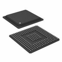
ADSP-BF535PBBZ-200 Analog Devices Inc, ADSP-BF535PBBZ-200 Datasheet - Page 11

ADSP-BF535PBBZ-200
Manufacturer Part Number
ADSP-BF535PBBZ-200
Description
200/400MMAC 16-bit DSP MICROCOMPUTER
Manufacturer
Analog Devices Inc
Series
Blackfin®r
Type
Fixed Pointr
Specifications of ADSP-BF535PBBZ-200
Interface
PCI, SPI, SSP, UART, USB
Clock Rate
200MHz
Non-volatile Memory
External
On-chip Ram
308kB
Voltage - I/o
3.30V
Voltage - Core
1.50V
Operating Temperature
-40°C ~ 85°C
Mounting Type
Surface Mount
Package / Case
260-BGA
Lead Free Status / RoHS Status
Lead free / RoHS Compliant
Available stocks
Company
Part Number
Manufacturer
Quantity
Price
Company:
Part Number:
ADSP-BF535PBBZ-200
Manufacturer:
Analog Devices Inc
Quantity:
10 000
includes support for 5 to 8 data bits; 1 or 2 stop bits; and none,
even, or odd parity. The UART ports support two modes of
operation.
Each UART port’s baud rate (see
error code generation and status, and interrupts are
programmable:
Autobaud detection is supported, in conjunction with the
general-purpose timer functions.
The capabilities of UART0 are further extended with support for
the Infrared Data Association (IrDA Serial Infrared Physical
Layer Link Specification (SIR) protocol.
Programmable Flags (PFX)
The ADSP-BF535 Blackfin processor has 16 bidirectional,
general-purpose I/O programmable flag (PF15–0) pins. The pro-
grammable flag pins have special functions for clock multiplier
selection, SROM boot mode, and SPI port operation. For more
information, see
Page 10
can be individually controlled by manipulation of the flag control,
status, and interrupt registers.
REV. A
PIO (Programmed I/O)—The processor sends or receives
data by writing or reading I/O-mapped UATX or UARX
registers, respectively. The data is double-buffered on
both transmit and receive.
DMA (Direct Memory Access)—The DMA controller
transfers both transmit and receive data. This reduces the
number and frequency of interrupts required to transfer
data to and from memory. Each UART has two dedicated
DMA channels, one for transmit and one for receive. The
DMA channels have lower priority than most DMA
channels because of their relatively low service rates.
Bit rates ranging from (f
per second
Data formats from 7 to 12 bits per frame
Both transmit and receive operations can be configured
to generate maskable interrupts to the processor.
Flag Direction Control Register—Specifies the direction
of each individual PFx pin as input or output.
Flag Control and Status Registers—Rather than forcing
the software to use a read-modify-write process to control
the setting of individual flags, the ADSP-BF535 Blackfin
processor employs a “write one to set” and “write one to
clear” mechanism that allows any combination of individ-
ual flags to be set or cleared in a single instruction, without
affecting the level of any other flags. Two control registers
are provided, one register is written to in order to set flag
values while another register is written to in order to clear
flag values. Reading the flag status register allows software
to interrogate the sense of the flags.
and
Figure 5. UART Clock Rate Calculation
Clock Signals on Page
Serial Peripheral Interface (SPI) Ports on
UART Clock Rate
SCLK
/1048576) to (f
Figure
13. Each programmable flag
=
---------------- -
16
f
SCLK
5), serial data format,
D
SCLK
/16) bits
–11–
Dynamic Power Management
The ADSP-BF535 Blackfin processor provides four operating
modes, each with a different performance/power dissipation
profile. In addition, dynamic power management provides the
control functions, with the appropriate external power regulation
capability to dynamically alter the processor core supply voltage,
further reducing power dissipation. Control of clocking to each
of the ADSP-BF535 Blackfin processor peripherals also reduces
power dissipation. See
settings for each mode.
Full On Operating Mode
– Maximum Performance
In the full on mode, the PLL is enabled, and is not bypassed,
providing the maximum operational frequency. This is the
normal execution state in which maximum performance can be
achieved. The processor core and all enabled peripherals run at
full speed.
Active Operating Mode
– Moderate Power Savings
In the active mode, the PLL is enabled, but bypassed. The input
clock (CLKIN) is used to generate the clocks for the processor
core (CCLK) and peripherals (SCLK). When the PLL is
bypassed, CCLK runs at one-half the CLKIN frequency. Signif-
icant power savings can be achieved with the processor running
at one-half the CLKIN frequency. In this mode, the PLL multi-
plication ratio can be changed by setting the appropriate values
in the SSEL fields of the PLL control register (PLL_CTL).
When in the active mode, system DMA access to appropriately
configured L1 memory is supported.
Sleep Operating Mode
– High Power Savings
The sleep mode reduces power dissipation by disabling the clock
to the processor core (CCLK). The PLL and system clock
(SCLK), however, continue to operate in this mode. Any inter-
rupt, typically via some external event or RTC activity, will wake
up the processor. When in sleep mode, assertion of any interrupt
will cause the processor to sense the value of the bypass bit
Flag Interrupt Mask Registers—The two flag interrupt
mask registers allow each individual PFx pin to function
as an interrupt to the processor. Similar to the two flag
control registers that are used to set and clear individual
flag values, one flag interrupt mask register sets bits to
enable interrupt function, and the other flag interrupt
mask register clears bits to disable interrupt function. PFx
pins defined as inputs can be configured to generate
hardware interrupts, while output PFx pins can be con-
figured to generate software interrupts.
Flag Interrupt Sensitivity Registers—The two flag
interrupt sensitivity registers specify whether individual
PFx pins are level- or edge-sensitive and specify (if edge-
sensitive) whether just the rising edge or both the rising
and falling edges of the signal are significant. One register
selects the type of sensitivity, and one register selects
which edges are significant for edge-sensitivity.
Table 3
for a summary of the power
ADSP-BF535


