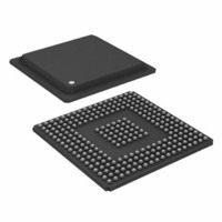
ADSP-BF535PBBZ-200 Analog Devices Inc, ADSP-BF535PBBZ-200 Datasheet - Page 36

ADSP-BF535PBBZ-200
Manufacturer Part Number
ADSP-BF535PBBZ-200
Description
200/400MMAC 16-bit DSP MICROCOMPUTER
Manufacturer
Analog Devices Inc
Series
Blackfin®r
Type
Fixed Pointr
Specifications of ADSP-BF535PBBZ-200
Interface
PCI, SPI, SSP, UART, USB
Clock Rate
200MHz
Non-volatile Memory
External
On-chip Ram
308kB
Voltage - I/o
3.30V
Voltage - Core
1.50V
Operating Temperature
-40°C ~ 85°C
Mounting Type
Surface Mount
Package / Case
260-BGA
Lead Free Status / RoHS Status
Lead free / RoHS Compliant
Available stocks
Company
Part Number
Manufacturer
Quantity
Price
Company:
Part Number:
ADSP-BF535PBBZ-200
Manufacturer:
Analog Devices Inc
Quantity:
10 000
ADSP-BF535
Output Drive Currents
Figure 19
acteristics for the output drivers of the ADSP-BF535 Blackfin
processor. The curves represent the current drive capability of
the output drivers as a function of output voltage.
applies to the ABE3–0, SDQM3–0, ADDR25–2, AMS3–0,
AOE, ARE, AWE, CLKOUT, SCLK1, DATA31–0, DT1–0,
EMU, MISO1–0, MOSI1–0, PF15–0, RFS1–0, RSCLK1–0,
SA10, SCAS, SCK1–0, SCKE, SCLK0, DEEPSLEEP,
SMS3–0, SRAS, SUSPEND, SWE, TDO, TFS1–0, TMR2–0,
TSCLK1–0, TX1–0, TXDMNS, TXDPLS, TXEN, and
XTAL0 pins.
PCI_CBE3–0, PCI_DEVSEL, PCI_FRAME, PCI_INTA,
PCI_IRDY, PCI_PAR, PCI_PERR, PCI_RST, PCI_SERR,
PCI_STOP, and PCI_TRDY pins.
PCI_REQ pin.
200
150
100
100
150
200
250
300
200
150
100
100
150
200
Figure 20. PCI 33 MHz Output Drive Current
50
50
50
50
0
0
through
0
0
V
V
OL
OL
V
Figure 20
V
Figure 19. Output Drive Current
OL
V
(V
(V
OL
OH
0.5
0.5
DDEXT
(V
DDEXT
(V
(V
DDEXT
Figure 21
DDEXT
V
DDEXT
OL
= 3.45V, 0°C)
= 3.45V,
1.0
1.0
V
(V
= 2.5V, +85°C)
OH
SOURCE (V
= 3.45V,
DDEXT
applies to the PCI_AD31–0,
= 3.45V,
V
V
SOURCE (V
V
OL
(V
OH
OH
DDEXT
(V
1.5
1.5
(V
(V
= 3.3V, +25°C)
DDEXT
45°C)
show typical current-voltage char-
V
DDEXT
DDEXT
V
OL
V
V
OH
40°C)
40°C)
= 3.45V,
OL
OH
O
(V
) VOLTAGE – V
2.0
O
(V
2.0
= 3.45V, 0°C)
V
(V
DDEXT
= 3.45V, 0°C)
(V
) VOLTAGE – V
V
= 3.45V, 0°C)
OL
DDEXT
V
Figure 21
OH
DDEXT
DDEXT
OH
(V
V
V
(V
(V
OH
DDEXT
OL
= 3.15V, +105°C)
2.5
2.5
45°C)
DDEXT
= 3.3V, +25°C)
DDEXT
= 3.15V, +105°C)
= 3.3V, +25°C)
(V
(V
V
DDEXT
DDEXT
= 3.3V, +25°C)
OH
= 3.15V, +105°C)
= 3.15V, +105°C)
3.0
3.0
applies to the
(V
= 2.5V, +85°C)
= 2.5V, +85°C)
DDEXT
+85°C)
Figure 19
3.5
3.5
= 2.5V,
4.0
4.0
–36–
Power Dissipation
Total power dissipation has two components: one due to internal
circuitry (P
drivers (P
circuitry (V
instruction execution sequence and the data operands involved.
Table 27
(PLL) circuitry (V
The external component of total power dissipation is caused by
the switching of output pins. Its magnitude depends on:
The external component is calculated using:
Table 26. Internal Power Dissipation
1
2
3
4
5
Parameter
I
I
I
I
I
I
I
Processor executing 75% dual Mac, 25% ADD with moderate data bus
Implementation of Enhanced Full Rate (EFR) GSM algorithm.
See the ADSP-BF535 Blackfin Processor Hardware Reference Manual for
DDTYP
DDEFR
DDSLEEP
DDDEEPSLEEP
DDRESET
DD
DD
activity.
definitions of Sleep and Deep Sleep operating modes.
Maximum frequency (f
switch during each cycle
Their load capacitance (C
Their voltage swing (V
is specified for when the device is in the reset state.
data is specified for typical process parameters. All data at 25ºC.
2
3
200
150
100
100
150
200
50
50
4
5
Figure 21. PCI_REQ Output Drive Current
0
shows the power dissipation for the phase-locked loop
EXT
0
DDINT
INT
).
4
V
) and one due to the switching of external output
Table 26
OL
Test Conditions
f
100 MHz
V
1.0 V
96.0
114.0
15.0
4.0
132.0
V
V
P
CCLK
OH
OH
0.5
). Internal power dissipation is dependent on the
DDINT
(V
EXT
V
(V
DDEXT
(V
OL
DDPLL
DDEXT
DDEXT
(V
=
=
DDEXT
1.0
=
= 3.45V, 0°C)
V
).
shows the power dissipation for internal
SOURCE (V
OH
V
= 3.45V,
= 2.5V, +85°C)
V
f
200 MHz
V
1.2 V
206.0
248.0
29.0
5.0
255.0
OL
DDEXT
CCLK
(V
= 3.45V,
DDEXT
DDINT
0
1.5
DDEXT
(V
) at which all output pins can
DDEXT
0
=
) of all switching pins
45°C)
2
1
O
)
= 3.45V, 0°C)
=
) VOLTAGE – V
2.0
V
45°C)
= 3.15V, +105°C)
V
OH
OL
V
f
300 MHz
V
1.5 V
387.0
463.0
52.0
8.2
485.3
OL
CCLK
(V
C
(V
DDINT
DDEXT
(V
DDEXT
0
2.5
DDEXT
V
=
OH
f
0
= 3.3V, +25°C)
= 2.5V, +85°C)
=
3.0
(V
= 3.3V, +25°C)
DDEXT
+105°C)
f
350 MHz
V
1.6 V
498.0
579.0
62.0
9.8
651.0
CCLK
DDINT
3.5
= 3.15V,
=
=
REV. A
4.0
Unit
mA
mA
mA
mA
mA


