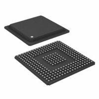
ADSP-BF535PBBZ-200 Analog Devices Inc, ADSP-BF535PBBZ-200 Datasheet - Page 12

ADSP-BF535PBBZ-200
Manufacturer Part Number
ADSP-BF535PBBZ-200
Description
200/400MMAC 16-bit DSP MICROCOMPUTER
Manufacturer
Analog Devices Inc
Series
Blackfin®r
Type
Fixed Pointr
Specifications of ADSP-BF535PBBZ-200
Interface
PCI, SPI, SSP, UART, USB
Clock Rate
200MHz
Non-volatile Memory
External
On-chip Ram
308kB
Voltage - I/o
3.30V
Voltage - Core
1.50V
Operating Temperature
-40°C ~ 85°C
Mounting Type
Surface Mount
Package / Case
260-BGA
Lead Free Status / RoHS Status
Lead free / RoHS Compliant
Available stocks
Company
Part Number
Manufacturer
Quantity
Price
Company:
Part Number:
ADSP-BF535PBBZ-200
Manufacturer:
Analog Devices Inc
Quantity:
10 000
ADSP-BF535
(BYPASS) in the PLL Control register (PLL_CTL). If bypass is
disabled, the processor transitions to the full on mode. If bypass
is enabled, the processor transitions to the Active mode.
When in Sleep mode, system DMA access to L1 memory is not
supported.
Deep Sleep Operating Mode
– Maximum Power Savings
The deep sleep mode maximizes power savings by disabling the
clocks to the processor core (CCLK) and to all synchronous
peripherals (SCLK). Asynchronous peripherals, such as the
RTC, may still be running but will not be able to access internal
resources or external memory. This powered down mode can
only be exited by assertion of the reset interrupt (RESET) or by
an asynchronous interrupt generated by the RTC. When in deep
sleep mode, assertion of RESET causes the processor to sense
the value of the BYPASS pin. If bypass is disabled, the processor
will transition to full on mode. If bypass is enabled, the processor
will transition to active mode. When in deep sleep mode,
assertion of the RTC asynchronous interrupt causes the
processor to transition to the full on mode, regardless of the value
of the BYPASS pin.
Power Savings
As shown in
supports five different power domains. The use of multiple power
domains maximizes flexibility, while maintaining compliance
with industry standards and conventions. By isolating the internal
logic of the ADSP-BF535 Blackfin processor into its own power
domain, separate from the PLL, RTC, PCI, and other I/O, the
processor can take advantage of dynamic power management,
without affecting the PLL, RTC, or other I/O devices.
Table
4, the ADSP-BF535 Blackfin processor
AND PDWN = 0
STOPCK = 1
ACTIVE
AND PLL_OFF = 0
AND BYPASS = 1
MSEL = NEW
PDWN = 1
WAKEUP AND
RTC_WAKEUP
BYPASS = 1
AND PLL_OFF = 0
AND STOPCK = 0
AND PDWN = 0
Figure 6. Mode Transitions
BYPASS = 0
HARDWARE
–12–
SLEEP
SLEEP
RESET
RESET
DEEP
The DEEPSLEEP output is asserted in this mode.
Mode Transitions
The available mode transitions diagrammed in
accomplished either by the interrupt events described in the
following sections or by programming the PLLCTL register with
the appropriate values and then executing the PLL programming
sequence.
This instruction sequence takes the processor to a known idle
state with the interrupts disabled. Note that all DMA activity
should be disabled during mode transitions.
Table 3. Operating Mode Power Settings
AND STOPCK = 0
Table 4. Power Domains
Mode
Full On
Active
Sleep
Deep +
AND PDWN = 0
Power Domain
All internal logic, except PLL and RTC
Analog PLL internal logic
RTC internal logic and crystal I/O
PCI I/O
All other I/O
BYPASS = 1
WAKEUP AND
BYPASS = 0
PDWN = 1
AND PLL_OFF = 0
PLL
Enabled No
Enabled Yes
Enabled Yes or No Disabled
Disabled
AND BYPASS = 0
MSEL = NEW
FULL-ON
AND PDWN = 0
STOPCK = 1
PLL
Bypassed
Core Clock
(CCLK)
Enabled
Enabled
Disabled
Figure 6
V
V
V
V
V
V
DD
DDINT
DDPLL
DDRTC
DDPCIEXT
DDEXT
System Clock
(SCLK)
Enabled
Enabled
Enabled
Disabled
Range
REV. A
are


