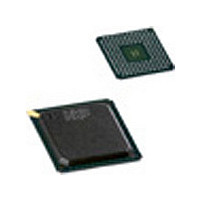
PNX1302EH NXP Semiconductors, PNX1302EH Datasheet - Page 261

PNX1302EH
Manufacturer Part Number
PNX1302EH
Description
Manufacturer
NXP Semiconductors
Datasheet
1.PNX1302EH.pdf
(548 pages)
Specifications of PNX1302EH
Lead Free Status / RoHS Status
Not Compliant
Available stocks
Company
Part Number
Manufacturer
Quantity
Price
Company:
Part Number:
PNX1302EH
Manufacturer:
NXP
Quantity:
201
Part Number:
PNX1302EH
Manufacturer:
PHILIPS/飞利浦
Quantity:
20 000
Company:
Part Number:
PNX1302EH,557
Manufacturer:
NXP Semiconductors
Quantity:
10 000
Company:
Part Number:
PNX1302EH/G
Manufacturer:
NXP
Quantity:
5 510
Part Number:
PNX1302EH/G
Manufacturer:
NXP/恩智浦
Quantity:
20 000
- Current page: 261 of 548
- Download datasheet (6Mb)
Philips Semiconductors
17.7
Depending on the settings of the TIE, RIE and CDE bits
in the SSI_CTL register, the SSI unit can generate inter-
rupts. This is best illustrated by
RXFES and TXFES are the internal receive and transmit
framing error conditions. When an SSI interrupt is detect-
ed, the interrupt service routine should check all status
bits.The interrupts should be set up as level-triggered in-
terrupts.
17.8
The SSI unit supports both access orders for the 16-bit
halves of a machine word. In addition, the shift direction
can be controlled to select MSB or LSB shifting first. The
SSI_CTL.EMS bit controls the 16-bit endian mode, and
Figure 17-8. Interrupt generation logic.
Figure 17-9. 16-bit endian and shift direction operation.
INTERRUPT GENERATION
16-BIT ENDIAN-NESS AND SHIFT
DIRECTION
EMS = 1, TSD = 0
EMS = 1, TSD = 1
EMS = 0, TSD = 1
EMS = 0, TSD = 0
TXFES
RXFES
TUE
TDE
ROE
RDF
SSI_TXDATA
SSI_TXDATA
SSI_TXDATA
SSI_TXDATA
SSI_RXFSX
SSI_RXFSX
SSI_RXFSX
SSI_RXFSX
Figure
or
or
SSI_TXDR
17-8. Note:
D16 D15 D14 D13 ....... D2
D31 D0
D0
D15 D16 D17 D18 ....... D29 D30 D31 D0
TIE
RIE
D31 D30 D29 ....... D18 D17 D16 D15 D14 D13 ....... D2
D1
31
and
and
D2
1
1
1
1
st
st
st
st
....... D13 D14 D15 D16 D17 D18 ....... D29 D30 D31 D0
CDE & CDS
word
word
word
word
the TSD and RSD bits control transmit and receive shift
direction.
When EMS is set, the first data word received in a frame
will be transferred to bit 15-0 of the SSI_RxDR, the sec-
ond word will be transferred to bits 31-16 of the
SSI_RxDR. EMS = ‘0’ reverses the order of the halves of
SSI_RxDR. Likewise in the transmitter, when EMS is set,
the first data word transmitted in a frame will be bits 15-
0 of SSI_TxDR, the second word transferred will be bits
31-16 of SSI_TxDR.
TSD and RSD control the shift direction of transmit and
receive shift registers (TxSR and RxSR). Transmit data
is transmitted MSB first when TSD is ‘0’ or LSB first oth-
erwise. Receive data is received MSB first when RSD
equals ‘0’, LSB first otherwise.
For an example of the transmit operation see
Figure
shifted in
PRELIMINARY SPECIFICATION
15
D1
D0
17-9. Receive works the same, only that data is
or
.
D31 D30 D29 ....... D18 D17 D16 D15 D14 D13 ......
0
D1
D2
2
2
nd
2
2
nd
nd
nd
....... D13 D14 D15 D16 D17 D18 ......
word
word
word
word
SSI interrupt
Synchronous Serial Interface
D1
D0
D31 D30 D29 ......
3
3
3
3
D1
th
th
th
th
word
word
word
word
D2
......
17-7
Related parts for PNX1302EH
Image
Part Number
Description
Manufacturer
Datasheet
Request
R
Part Number:
Description:
NXP Semiconductors designed the LPC2420/2460 microcontroller around a 16-bit/32-bitARM7TDMI-S CPU core with real-time debug interfaces that include both JTAG andembedded trace
Manufacturer:
NXP Semiconductors
Datasheet:

Part Number:
Description:
NXP Semiconductors designed the LPC2458 microcontroller around a 16-bit/32-bitARM7TDMI-S CPU core with real-time debug interfaces that include both JTAG andembedded trace
Manufacturer:
NXP Semiconductors
Datasheet:
Part Number:
Description:
NXP Semiconductors designed the LPC2468 microcontroller around a 16-bit/32-bitARM7TDMI-S CPU core with real-time debug interfaces that include both JTAG andembedded trace
Manufacturer:
NXP Semiconductors
Datasheet:
Part Number:
Description:
NXP Semiconductors designed the LPC2470 microcontroller, powered by theARM7TDMI-S core, to be a highly integrated microcontroller for a wide range ofapplications that require advanced communications and high quality graphic displays
Manufacturer:
NXP Semiconductors
Datasheet:
Part Number:
Description:
NXP Semiconductors designed the LPC2478 microcontroller, powered by theARM7TDMI-S core, to be a highly integrated microcontroller for a wide range ofapplications that require advanced communications and high quality graphic displays
Manufacturer:
NXP Semiconductors
Datasheet:
Part Number:
Description:
The Philips Semiconductors XA (eXtended Architecture) family of 16-bit single-chip microcontrollers is powerful enough to easily handle the requirements of high performance embedded applications, yet inexpensive enough to compete in the market for hi
Manufacturer:
NXP Semiconductors
Datasheet:
Part Number:
Description:
The XA-S3 device is a member of Philips Semiconductors? XA(eXtended Architecture) family of high performance 16-bitsingle-chip microcontrollers
Manufacturer:
NXP Semiconductors
Datasheet:

Part Number:
Description:
The NXP BlueStreak LH75401/LH75411 family consists of two low-cost 16/32-bit System-on-Chip (SoC) devices
Manufacturer:
NXP Semiconductors
Datasheet:

Part Number:
Description:
The NXP LPC3130/3131 combine an 180 MHz ARM926EJ-S CPU core, high-speed USB2
Manufacturer:
NXP Semiconductors
Datasheet:

Part Number:
Description:
The NXP LPC3141 combine a 270 MHz ARM926EJ-S CPU core, High-speed USB 2
Manufacturer:
NXP Semiconductors

Part Number:
Description:
The NXP LPC3143 combine a 270 MHz ARM926EJ-S CPU core, High-speed USB 2
Manufacturer:
NXP Semiconductors

Part Number:
Description:
The NXP LPC3152 combines an 180 MHz ARM926EJ-S CPU core, High-speed USB 2
Manufacturer:
NXP Semiconductors

Part Number:
Description:
The NXP LPC3154 combines an 180 MHz ARM926EJ-S CPU core, High-speed USB 2
Manufacturer:
NXP Semiconductors

Part Number:
Description:
Standard level N-channel enhancement mode Field-Effect Transistor (FET) in a plastic package using NXP High-Performance Automotive (HPA) TrenchMOS technology
Manufacturer:
NXP Semiconductors
Datasheet:


