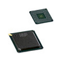
PNX1302EH NXP Semiconductors, PNX1302EH Datasheet - Page 292

PNX1302EH
Manufacturer Part Number
PNX1302EH
Description
Manufacturer
NXP Semiconductors
Datasheet
1.PNX1302EH.pdf
(548 pages)
Specifications of PNX1302EH
Lead Free Status / RoHS Status
Not Compliant
Available stocks
Company
Part Number
Manufacturer
Quantity
Price
Company:
Part Number:
PNX1302EH
Manufacturer:
NXP
Quantity:
201
Part Number:
PNX1302EH
Manufacturer:
PHILIPS/飞利浦
Quantity:
20 000
Company:
Part Number:
PNX1302EH,557
Manufacturer:
NXP Semiconductors
Quantity:
10 000
Company:
Part Number:
PNX1302EH/G
Manufacturer:
NXP
Quantity:
5 510
Part Number:
PNX1302EH/G
Manufacturer:
NXP/恩智浦
Quantity:
20 000
- Current page: 292 of 548
- Download datasheet (6Mb)
PNX1300/01/02/11 Data Book
A table of PCI-XIO Bus Clock frequencies versus Clock
field values is shown in
PCI_CLK operating frequency should be set to observe
the frequency limits given in the AC/DC timing character-
ization data for PNX1300. Odd values of ‘Clock Frequen-
cy’ are recommended, resulting in an even divider, which
generates a 50% duty cycle PCI_CLK.
22.5.2
The XIO Bus controller has an automatic wait state gen-
erator to allow for read and write cycle times of devices
on the XIO bus.
Table 22-4. Wait state generator codes
22-8
Figure 22-10. PCI-XIO Bus timing: single byte read, 0 wait states
PCI_AD[31:24]: DATA
PCI_AD[23:0]: ADDR
PCI_C/BE1#/IOWR#
PCI_C/BE0#/IORD#
Read Sample Point
PCI_C/BE2#/DS#
PCI_INTB#/CE#
PCI_DEVSEL#
Code
PCI_FRAME#
...
PCI_TRDY#
Wait State Generator
0
1
2
7
PCI_IRDY#
PCI_CLK
PRELIMINARY SPECIFICATION
Table
Frame Time
Wait States
22-3. Note that the
PCI Command
PCI Address
PCI Address
PCI Command
PCI Command
...
0
1
2
7
Bus Turnaround
& Address Setup
22.6
The timing for the PCI-XIO bus is shown below: Note that
the ‘fat’ lines indicate active drive by PNX1300. Thin lines
indicate areas where the PNX1300 is not actively driving.
(In these areas, pull-up resistors retain the signal high for
control signals, PCI_AD lines are left floating.)
Figure 22-10
transfer.
read transfer with wait states.
timing for a DMA burst read transfer of 2 bytes, and
Figure 22-16
transfer of 2 bytes. The DMA burst transfers are shown
at maximum rate, with zero wait states. DMA burst trans-
fers with wait states insert wait states between the trans-
fers. In the read case, the IORD# enable and DS# are ex-
tended by the wait states. In the write case, the IOWR#
enable and DS# are delayed by the wait states.
XIO Addrs
XIO Transfer
PCI-XIO BUS TIMING
Figure 22-11
Read Data
shows the timing for a single byte read
shows the timing for a DMA burst write
shows the timing for a single byte
Bus Idle
Philips Semiconductors
Figure 22-14
shows the
Related parts for PNX1302EH
Image
Part Number
Description
Manufacturer
Datasheet
Request
R
Part Number:
Description:
NXP Semiconductors designed the LPC2420/2460 microcontroller around a 16-bit/32-bitARM7TDMI-S CPU core with real-time debug interfaces that include both JTAG andembedded trace
Manufacturer:
NXP Semiconductors
Datasheet:

Part Number:
Description:
NXP Semiconductors designed the LPC2458 microcontroller around a 16-bit/32-bitARM7TDMI-S CPU core with real-time debug interfaces that include both JTAG andembedded trace
Manufacturer:
NXP Semiconductors
Datasheet:
Part Number:
Description:
NXP Semiconductors designed the LPC2468 microcontroller around a 16-bit/32-bitARM7TDMI-S CPU core with real-time debug interfaces that include both JTAG andembedded trace
Manufacturer:
NXP Semiconductors
Datasheet:
Part Number:
Description:
NXP Semiconductors designed the LPC2470 microcontroller, powered by theARM7TDMI-S core, to be a highly integrated microcontroller for a wide range ofapplications that require advanced communications and high quality graphic displays
Manufacturer:
NXP Semiconductors
Datasheet:
Part Number:
Description:
NXP Semiconductors designed the LPC2478 microcontroller, powered by theARM7TDMI-S core, to be a highly integrated microcontroller for a wide range ofapplications that require advanced communications and high quality graphic displays
Manufacturer:
NXP Semiconductors
Datasheet:
Part Number:
Description:
The Philips Semiconductors XA (eXtended Architecture) family of 16-bit single-chip microcontrollers is powerful enough to easily handle the requirements of high performance embedded applications, yet inexpensive enough to compete in the market for hi
Manufacturer:
NXP Semiconductors
Datasheet:
Part Number:
Description:
The XA-S3 device is a member of Philips Semiconductors? XA(eXtended Architecture) family of high performance 16-bitsingle-chip microcontrollers
Manufacturer:
NXP Semiconductors
Datasheet:

Part Number:
Description:
The NXP BlueStreak LH75401/LH75411 family consists of two low-cost 16/32-bit System-on-Chip (SoC) devices
Manufacturer:
NXP Semiconductors
Datasheet:

Part Number:
Description:
The NXP LPC3130/3131 combine an 180 MHz ARM926EJ-S CPU core, high-speed USB2
Manufacturer:
NXP Semiconductors
Datasheet:

Part Number:
Description:
The NXP LPC3141 combine a 270 MHz ARM926EJ-S CPU core, High-speed USB 2
Manufacturer:
NXP Semiconductors

Part Number:
Description:
The NXP LPC3143 combine a 270 MHz ARM926EJ-S CPU core, High-speed USB 2
Manufacturer:
NXP Semiconductors

Part Number:
Description:
The NXP LPC3152 combines an 180 MHz ARM926EJ-S CPU core, High-speed USB 2
Manufacturer:
NXP Semiconductors

Part Number:
Description:
The NXP LPC3154 combines an 180 MHz ARM926EJ-S CPU core, High-speed USB 2
Manufacturer:
NXP Semiconductors

Part Number:
Description:
Standard level N-channel enhancement mode Field-Effect Transistor (FET) in a plastic package using NXP High-Performance Automotive (HPA) TrenchMOS technology
Manufacturer:
NXP Semiconductors
Datasheet:


