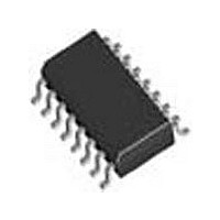
SI3018-F-FSR Silicon Laboratories Inc, SI3018-F-FSR Datasheet - Page 76

SI3018-F-FSR
Manufacturer Part Number
SI3018-F-FSR
Description
Modem Chip Chipset 16-Pin SOIC T/R
Manufacturer
Silicon Laboratories Inc
Datasheet
1.SI3018-F-FSR.pdf
(112 pages)
Specifications of SI3018-F-FSR
Package
16SOIC
Main Category
Chipset
Sub-category
Data/Voice
Typical Operating Supply Voltage
3.3 V
Power Supply Type
Digital
Typical Supply Current
8.5 mA
Minimum Operating Supply Voltage
3 V
Maximum Operating Supply Voltage
3.6 V
Data Rate
54.6875Kbps
Operating Supply Voltage (typ)
3.3V
Operating Supply Voltage (min)
3V
Operating Supply Voltage (max)
3.6V
Operating Temp Range
0C to 70C
Operating Temperature Classification
Commercial
Pin Count
16
Mounting
Surface Mount
Lead Free Status / Rohs Status
Compliant
Available stocks
Company
Part Number
Manufacturer
Quantity
Price
Company:
Part Number:
SI3018-F-FSR
Manufacturer:
SiliconL
Quantity:
52 026
Company:
Part Number:
SI3018-F-FSR
Manufacturer:
SILICON
Quantity:
57
Part Number:
SI3018-F-FSR
Manufacturer:
SILICONLABS/芯科
Quantity:
20 000
Si3050 + Si3018/19
Register 22. Ring Validation Control 1
Reset settings = 1001_0110
76
Bit
7:6
5:0
Name
Type
Bit
RDLY[1:0]
RMX[5:0]
Name
D7
RDLY[1:0]
Ring Delay Bits 1 and 0.
These bits, in combination with the RDLY[2] bit (Register 23), set the amount of time
between when a ring signal is validated and when a valid ring signal is indicated.
RDLY[2]
Ring Assertion Maximum Count.
These bits set the maximum ring frequency for a valid ring signal within a 10% margin of
error. During ring qualification, a timer is loaded with the RAS[5:0] field upon a TIP/RING
event and decrements at a regular rate. When a subsequent TIP/RING event occurs, the
timer value is compared to the RMX[5:0] field and if it exceeds the value in RMX[5:0] then
the frequency of the ring is too high and the ring is invalidated. The difference between
RAS[5:0] and RMX[5:0] identifies the minimum duration between TIP/RING events to qual-
ify as a ring, in binary-coded increments of 2.0 ms (nominal). A TIP/RING event typically
occurs twice per ring tone period. At 20 Hz, TIP/RING events would occur every 1/
(2 x 20 Hz) = 25 ms. To calculate the correct RMX[5:0] value for a frequency range [f_min,
f_max], the following equation should be used:
To compensate for error margin and ensure a sufficient ring detection window, it is recom-
mended that the calculated value of RMX[5:0] be incremented by 1.
R/W
...
0
0
0
1
D6
RDLY[1:0]
RMX 5:0
10
00
11
D5
01
Rev. 1.31
RAS 5:0
Delay
1792 ms
256 ms
512 ms
D4
0 ms
Function
–
-------------------------------------------- - RMX RAS
2 f_max
D3
RMX[5:0]
1
R/W
2 ms
D2
D1
D0


