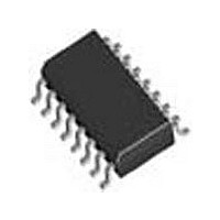
SI3018-F-FSR Silicon Laboratories Inc, SI3018-F-FSR Datasheet - Page 96

SI3018-F-FSR
Manufacturer Part Number
SI3018-F-FSR
Description
Modem Chip Chipset 16-Pin SOIC T/R
Manufacturer
Silicon Laboratories Inc
Datasheet
1.SI3018-F-FSR.pdf
(112 pages)
Specifications of SI3018-F-FSR
Package
16SOIC
Main Category
Chipset
Sub-category
Data/Voice
Typical Operating Supply Voltage
3.3 V
Power Supply Type
Digital
Typical Supply Current
8.5 mA
Minimum Operating Supply Voltage
3 V
Maximum Operating Supply Voltage
3.6 V
Data Rate
54.6875Kbps
Operating Supply Voltage (typ)
3.3V
Operating Supply Voltage (min)
3V
Operating Supply Voltage (max)
3.6V
Operating Temp Range
0C to 70C
Operating Temperature Classification
Commercial
Pin Count
16
Mounting
Surface Mount
Lead Free Status / Rohs Status
Compliant
Available stocks
Company
Part Number
Manufacturer
Quantity
Price
Company:
Part Number:
SI3018-F-FSR
Manufacturer:
SiliconL
Quantity:
52 026
Company:
Part Number:
SI3018-F-FSR
Manufacturer:
SILICON
Quantity:
57
Part Number:
SI3018-F-FSR
Manufacturer:
SILICONLABS/芯科
Quantity:
20 000
Si3050 + Si3018/19
Register 59. Spark Quenching Control
Reset settings = xxxx_xxxx
96
Name
Bit
Type
7
6
5
4
3
2
1
0
Bit
Reserved Always write this bit to zero.
Reserved Always write this bit to zero.
Reserved Always write this bit to zero.
Reserved Always write this bit to zero.
Name
GCE
RG1
SQ1
SQ0
D7
Spark Quenching.
This bit, in combination with the OHS bit (Register 16), and the OHS2 bit (Register 31), sets
the amount of time for the line-side device to go on-hook. The on-hook speeds specified are
measured from the time the OH bit is cleared until loop current equals zero.
OHS
Spark Quenching.
This bit, in combination with the OHS bit (Register 16), and the OHS2 bit (Register 31), sets
the amount of time for the line-side device to go on-hook. The on-hook speeds specified are
measured from the time the OH bit is cleared until loop current equals zero.
OHS
Receive Gain 1 (Line-side Revision E or later).
This bit enables receive path gain adjustment.
0 = No gain applied to hybrid, full scale RX on line = 0 dBm.
1 = 1 dB of gain applied to hybrid, full scale RX on line = –1 dBm.
Guarded Clear Enable (Line-side Revision E or later).
This bit (in conjunction with the R2 bit set to 1) enables the Si3050 to meet BT’s Guarded
Clear Spec (B5 6450, Part 1: 1993, Section 15.4.3.3). With these bits set, the DAA will draw
approximately 2.5 mA of current from the line while on-hook.
0 = Default, DAA does not draw loop current.
1 = Guarded Clear enabled, DAA draws 2.5 mA while on-hook to meet Guarded Clear
requirement.
0
0
1
0
0
1
SQ1
R/W
D6
OHS2
OHS2
0
1
X
0
1
X
D5
SQ[1:0]
SQ[1:0]
00
00
11
00
00
11
Rev. 1.31
SQ0
R/W
D4
Mean On-Hook Speed
Less than 0.5 ms
3 ms±10% (meets ETSI standard)
26 ms ±10% (meets Australia spark quenching spec)
Mean On-Hook Speed
Less than 0.5 ms
3 ms±10% (meets ETSI standard)
26 ms ±10% (meets Australia spark quenching spec)
Function
D3
RG1
R/W
D2
GCE
R/W
D1
D0


