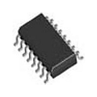
SI3018-F-FSR Silicon Laboratories Inc, SI3018-F-FSR Datasheet - Page 86

SI3018-F-FSR
Manufacturer Part Number
SI3018-F-FSR
Description
Modem Chip Chipset 16-Pin SOIC T/R
Manufacturer
Silicon Laboratories Inc
Datasheet
1.SI3018-F-FSR.pdf
(112 pages)
Specifications of SI3018-F-FSR
Package
16SOIC
Main Category
Chipset
Sub-category
Data/Voice
Typical Operating Supply Voltage
3.3 V
Power Supply Type
Digital
Typical Supply Current
8.5 mA
Minimum Operating Supply Voltage
3 V
Maximum Operating Supply Voltage
3.6 V
Data Rate
54.6875Kbps
Operating Supply Voltage (typ)
3.3V
Operating Supply Voltage (min)
3V
Operating Supply Voltage (max)
3.6V
Operating Temp Range
0C to 70C
Operating Temperature Classification
Commercial
Pin Count
16
Mounting
Surface Mount
Lead Free Status / Rohs Status
Compliant
Available stocks
Company
Part Number
Manufacturer
Quantity
Price
Company:
Part Number:
SI3018-F-FSR
Manufacturer:
SiliconL
Quantity:
52 026
Company:
Part Number:
SI3018-F-FSR
Manufacturer:
SILICON
Quantity:
57
Part Number:
SI3018-F-FSR
Manufacturer:
SILICONLABS/芯科
Quantity:
20 000
Si3050 + Si3018/19
Register 37. PCM Receive Start Count—High Byte
Reset settings = 0000_0000
Register 38. TX Gain Control 2
Reset settings = 0000_0000
86
Bit
7:2
1:0
Bit
7:5
3:0
4
Name
Name
Type
Type
Bit
Bit
TXG2[3:0] Transmit Gain 2.
Reserved Read returns zero.
Reserved
Name
RXS[1:0]
TGA2
Name
D7
D7
Transmit Gain or Attenuation 2.
0 = Incrementing the TXG2[3:0] bits results in gaining up the transmit path.
1 = Incrementing the TXG2[3:0] bits results in attenuating the transmit path.
Each bit increment represents 1 dB of gain or attenuation, up to a maximum of +12 dB and
–15 dB respectively.
For example:
TGA2
X
0
0
0
1
1
1
PCM Receive Start Count.
PCM Receive Start Count equals the number of PCLKs following FSYNC before data
reception begins.
Read returns zero.
D6
D6
TXG2[3:0]
0000
0001
11xx
0001
1111
:
:
D5
D5
Rev. 1.31
0 dB gain or attenuation is applied to the transmit path.
1 dB gain is applied to the transmit path.
12 dB gain is applied to the transmit path.
1 dB attenuation is applied to the transmit path.
15 dB attenuation is applied to the transmit path.
Result
TGA2
R/W
D4
D4
Function
Function
D3
D3
D2
D2
TXG2[3:0]
R/W
D1
D1
RXS[1:0]
R/W
D0
D0


