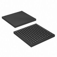
EP4CGX15BF14C8N Altera, EP4CGX15BF14C8N Datasheet - Page 138

EP4CGX15BF14C8N
Manufacturer Part Number
EP4CGX15BF14C8N
Description
IC CYCLONE IV FPGA 15K 169FBGA
Manufacturer
Altera
Series
CYCLONE® IV GXr
Datasheets
1.EP4CGX15BN11C8N.pdf
(44 pages)
2.EP4CGX15BN11C8N.pdf
(14 pages)
3.EP4CGX15BN11C8N.pdf
(478 pages)
4.EP4CGX15BN11C8N.pdf
(10 pages)
Specifications of EP4CGX15BF14C8N
Number Of Logic Elements/cells
14400
Number Of Labs/clbs
900
Total Ram Bits
540000
Number Of I /o
72
Voltage - Supply
1.16 V ~ 1.24 V
Mounting Type
Surface Mount
Operating Temperature
0°C ~ 85°C
Package / Case
169-FBGA
Lead Free Status / RoHS Status
Lead free / RoHS Compliant
Number Of Gates
-
Other names
544-1475
Available stocks
Company
Part Number
Manufacturer
Quantity
Price
Company:
Part Number:
EP4CGX15BF14C8N
Manufacturer:
ALTERA33
Quantity:
276
- EP4CGX15BN11C8N PDF datasheet
- EP4CGX15BN11C8N PDF datasheet #2
- EP4CGX15BN11C8N PDF datasheet #3
- EP4CGX15BN11C8N PDF datasheet #4
- Current page: 138 of 478
- Download datasheet (13Mb)
6–30
Figure 6–14. BLVDS Topology with Cyclone IV Devices Transmitters and Receivers
Cyclone IV Device Handbook, Volume 1
100 kΩ
100 kΩ
GND
f
f
R
1
T
V
CC
Figure 6–14
pairs.
The BLVDS I/O standard is supported on the top, bottom, and right I/O banks of
Cyclone IV devices. The BLVDS transmitter uses two single-ended output buffers
with the second output buffer programmed as inverted, while the BLVDS receiver
uses a true LVDS input buffer. The transmitter and receiver share the same pins. An
output-enabled (OE) signal is required to tristate the output buffers when the LVDS
input buffer receives a signal.
For more information, refer to the
Designing with BLVDS
The BLVDS bidirectional communication requires termination at both ends of the bus
in BLVDS. The termination resistor (R
which in turn depends on the loading on the bus. Increasing the load decreases the
bus differential impedance. With termination at both ends of the bus, termination is
not required between the two signals at the input buffer. A single series resistor (R
required at the output buffer to match the output buffer impedance to the
transmission line impedance. However, this series resistor affects the voltage swing at
the input buffer. The maximum data rate achievable depends on many factors.
Altera recommends that you perform simulation using the IBIS model while
considering factors such as bus loading, termination values, and output and input
buffer location on the bus to ensure that the required performance is achieved.
For more information about BLVDS interface support in Altera devices, refer to
AN 522: Implementing Bus LVDS Interface in Supported Altera Device
50 Ω
50
Ω
Output
Data
shows a typical BLVDS topology with multiple transmitter and receiver
Input
Data
50 Ω
50 Ω
Output
Data
Cyclone IV Device Datasheet
Input
Data
T
) must match the bus differential impedance,
50 Ω
50 Ω
Output
Data
Chapter 6: I/O Features in Cyclone IV Devices
© December 2010 Altera Corporation
Input
Data
50 Ω
50 Ω
High-Speed I/O Standards Support
chapter.
Families.
V
CC
100 kΩ
100 k
GND
R
T
Ω
S
) is
Related parts for EP4CGX15BF14C8N
Image
Part Number
Description
Manufacturer
Datasheet
Request
R

Part Number:
Description:
CYCLONE II STARTER KIT EP2C20N
Manufacturer:
Altera
Datasheet:

Part Number:
Description:
CPLD, EP610 Family, ECMOS Process, 300 Gates, 16 Macro Cells, 16 Reg., 16 User I/Os, 5V Supply, 35 Speed Grade, 24DIP
Manufacturer:
Altera Corporation
Datasheet:

Part Number:
Description:
CPLD, EP610 Family, ECMOS Process, 300 Gates, 16 Macro Cells, 16 Reg., 16 User I/Os, 5V Supply, 15 Speed Grade, 24DIP
Manufacturer:
Altera Corporation
Datasheet:

Part Number:
Description:
Manufacturer:
Altera Corporation
Datasheet:

Part Number:
Description:
CPLD, EP610 Family, ECMOS Process, 300 Gates, 16 Macro Cells, 16 Reg., 16 User I/Os, 5V Supply, 30 Speed Grade, 24DIP
Manufacturer:
Altera Corporation
Datasheet:

Part Number:
Description:
High-performance, low-power erasable programmable logic devices with 8 macrocells, 10ns
Manufacturer:
Altera Corporation
Datasheet:

Part Number:
Description:
High-performance, low-power erasable programmable logic devices with 8 macrocells, 7ns
Manufacturer:
Altera Corporation
Datasheet:

Part Number:
Description:
Classic EPLD
Manufacturer:
Altera Corporation
Datasheet:

Part Number:
Description:
High-performance, low-power erasable programmable logic devices with 8 macrocells, 10ns
Manufacturer:
Altera Corporation
Datasheet:

Part Number:
Description:
Manufacturer:
Altera Corporation
Datasheet:

Part Number:
Description:
Manufacturer:
Altera Corporation
Datasheet:

Part Number:
Description:
Manufacturer:
Altera Corporation
Datasheet:

Part Number:
Description:
CPLD, EP610 Family, ECMOS Process, 300 Gates, 16 Macro Cells, 16 Reg., 16 User I/Os, 5V Supply, 25 Speed Grade, 24DIP
Manufacturer:
Altera Corporation
Datasheet:


