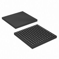
EP4CGX15BF14C8N Altera, EP4CGX15BF14C8N Datasheet - Page 154

EP4CGX15BF14C8N
Manufacturer Part Number
EP4CGX15BF14C8N
Description
IC CYCLONE IV FPGA 15K 169FBGA
Manufacturer
Altera
Series
CYCLONE® IV GXr
Datasheets
1.EP4CGX15BN11C8N.pdf
(44 pages)
2.EP4CGX15BN11C8N.pdf
(14 pages)
3.EP4CGX15BN11C8N.pdf
(478 pages)
4.EP4CGX15BN11C8N.pdf
(10 pages)
Specifications of EP4CGX15BF14C8N
Number Of Logic Elements/cells
14400
Number Of Labs/clbs
900
Total Ram Bits
540000
Number Of I /o
72
Voltage - Supply
1.16 V ~ 1.24 V
Mounting Type
Surface Mount
Operating Temperature
0°C ~ 85°C
Package / Case
169-FBGA
Lead Free Status / RoHS Status
Lead free / RoHS Compliant
Number Of Gates
-
Other names
544-1475
Available stocks
Company
Part Number
Manufacturer
Quantity
Price
Company:
Part Number:
EP4CGX15BF14C8N
Manufacturer:
ALTERA33
Quantity:
276
- EP4CGX15BN11C8N PDF datasheet
- EP4CGX15BN11C8N PDF datasheet #2
- EP4CGX15BN11C8N PDF datasheet #3
- EP4CGX15BN11C8N PDF datasheet #4
- Current page: 154 of 478
- Download datasheet (13Mb)
7–6
Table 7–2. Cyclone IV E Device DQS and DQ Bus Mode Support for Each Side of the Device
Cyclone IV Device Handbook, Volume 1
EP4CE30
EP4CE115
EP4CE40
EP4CE55
EP4CE75
Notes to
(1) The number of the DQS/DQ group is still preliminary.
(2) Some of the DQ pins can be used as RUP and RDN pins. You cannot use these groups if you are using these pins as RUP and RDN pins for
(3) Some of the DQ pins can be used as RUP pins while the DM pins can be used as RDN pins. You cannot use these groups if you are using the
(4) There is no DM pin support for these groups.
(5) PLLCLKOUT3n and PLLCLKOUT3p pins are shared with the DQ or DM pins to gain ×8 DQ group. You cannot use these groups if you are
Device
OCT calibration.
RUP and RDN pins for OCT calibration.
using PLLCLKOUT3n and PLLCLKOUT3p.
Table
f
7–2:
484-pin FBGA
780-pin FBGA
484-pin UBGA
484-pin FBGA
780-pin FBGA
For more information about device package outline, refer to the
Specifications
DQS pins are listed in the Cyclone IV pin tables as DQSXY, in which X indicates the
DQS grouping number and Y indicates whether the group is located on the top (T),
bottom (B), or right (R) side of the device. Similarly, the corresponding DQ pins are
marked as DQXY, in which the X denotes the DQ grouping number and Y denotes
whether the group is located on the top (T), bottom (B), or right (R) side of the device.
For example, DQS2T indicates a DQS pin belonging to group 2, located on the top side
of the device. Similarly, the DQ pins belonging to that group is shown as DQ2T.
Package
webpage.
Left
Right
Bottom
Top
Left
Right
Bottom
Top
Left
Right
Bottom
Top
Left
Right
Bottom
Top
Left
Right
Bottom
Top
Side
Number
Groups
×8
4
4
4
4
4
4
6
6
4
4
4
4
4
4
4
4
4
4
6
6
Chapter 7: External Memory Interfaces in Cyclone IV Devices
Number
Groups
×9
4
4
4
4
4
4
6
6
4
4
4
4
4
4
4
4
4
4
6
6
Cyclone IV Devices Memory Interfaces Pin Support
Number
Groups
×16
2
2
2
2
2
2
2
2
2
2
2
2
2
2
2
2
2
2
2
2
© December 2010 Altera Corporation
(Note 1)
Number
Groups
×18
2
2
2
2
2
2
2
2
2
2
2
2
2
2
2
2
2
2
2
2
Device Packaging
(Part 3 of 3)
Number
Groups
×32
1
1
1
1
1
1
1
1
1
1
1
1
1
1
1
1
1
1
1
1
Number
Groups
×36
1
1
1
1
1
1
1
1
1
1
1
1
1
1
1
1
1
1
1
1
Related parts for EP4CGX15BF14C8N
Image
Part Number
Description
Manufacturer
Datasheet
Request
R

Part Number:
Description:
CYCLONE II STARTER KIT EP2C20N
Manufacturer:
Altera
Datasheet:

Part Number:
Description:
CPLD, EP610 Family, ECMOS Process, 300 Gates, 16 Macro Cells, 16 Reg., 16 User I/Os, 5V Supply, 35 Speed Grade, 24DIP
Manufacturer:
Altera Corporation
Datasheet:

Part Number:
Description:
CPLD, EP610 Family, ECMOS Process, 300 Gates, 16 Macro Cells, 16 Reg., 16 User I/Os, 5V Supply, 15 Speed Grade, 24DIP
Manufacturer:
Altera Corporation
Datasheet:

Part Number:
Description:
Manufacturer:
Altera Corporation
Datasheet:

Part Number:
Description:
CPLD, EP610 Family, ECMOS Process, 300 Gates, 16 Macro Cells, 16 Reg., 16 User I/Os, 5V Supply, 30 Speed Grade, 24DIP
Manufacturer:
Altera Corporation
Datasheet:

Part Number:
Description:
High-performance, low-power erasable programmable logic devices with 8 macrocells, 10ns
Manufacturer:
Altera Corporation
Datasheet:

Part Number:
Description:
High-performance, low-power erasable programmable logic devices with 8 macrocells, 7ns
Manufacturer:
Altera Corporation
Datasheet:

Part Number:
Description:
Classic EPLD
Manufacturer:
Altera Corporation
Datasheet:

Part Number:
Description:
High-performance, low-power erasable programmable logic devices with 8 macrocells, 10ns
Manufacturer:
Altera Corporation
Datasheet:

Part Number:
Description:
Manufacturer:
Altera Corporation
Datasheet:

Part Number:
Description:
Manufacturer:
Altera Corporation
Datasheet:

Part Number:
Description:
Manufacturer:
Altera Corporation
Datasheet:

Part Number:
Description:
CPLD, EP610 Family, ECMOS Process, 300 Gates, 16 Macro Cells, 16 Reg., 16 User I/Os, 5V Supply, 25 Speed Grade, 24DIP
Manufacturer:
Altera Corporation
Datasheet:


