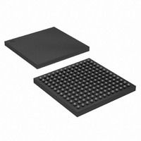
EP4CGX15BF14C8N Altera, EP4CGX15BF14C8N Datasheet - Page 194

EP4CGX15BF14C8N
Manufacturer Part Number
EP4CGX15BF14C8N
Description
IC CYCLONE IV FPGA 15K 169FBGA
Manufacturer
Altera
Series
CYCLONE® IV GXr
Datasheets
1.EP4CGX15BN11C8N.pdf
(44 pages)
2.EP4CGX15BN11C8N.pdf
(14 pages)
3.EP4CGX15BN11C8N.pdf
(478 pages)
4.EP4CGX15BN11C8N.pdf
(10 pages)
Specifications of EP4CGX15BF14C8N
Number Of Logic Elements/cells
14400
Number Of Labs/clbs
900
Total Ram Bits
540000
Number Of I /o
72
Voltage - Supply
1.16 V ~ 1.24 V
Mounting Type
Surface Mount
Operating Temperature
0°C ~ 85°C
Package / Case
169-FBGA
Lead Free Status / RoHS Status
Lead free / RoHS Compliant
Number Of Gates
-
Other names
544-1475
Available stocks
Company
Part Number
Manufacturer
Quantity
Price
Company:
Part Number:
EP4CGX15BF14C8N
Manufacturer:
ALTERA33
Quantity:
276
- EP4CGX15BN11C8N PDF datasheet
- EP4CGX15BN11C8N PDF datasheet #2
- EP4CGX15BN11C8N PDF datasheet #3
- EP4CGX15BN11C8N PDF datasheet #4
- Current page: 194 of 478
- Download datasheet (13Mb)
8–28
Figure 8–10. AP Configuration with Multiple Bus Masters
Notes to
(1) Connect the pull-up resistors to the V
(2) The nCEO pin is left unconnected or used as a user I/O pin when it does not feed the nCE pin of another device.
(3) The MSEL pin settings vary for different configuration voltage standards and POR time. To connect MSEL[3..0], refer to
(4) The AP configuration ignores the WAIT signal during configuration mode. However, if you are accessing flash during user mode with user logic,
(5) When cascading Cyclone IV E devices in a multi-device AP configuration, connect the repeater buffers between the master device and slave
(6) The other master device must fit the maximum overshoot equation outlined in
(7) The other master device can control the AP configuration bus by driving the nCE to high with an output high on the I/O pin.
(8) The other master device can pulse nCONFIG if it is under system control and not tied to V
Cyclone IV Device Handbook, Volume 1
page
you can optionally use the normal I/O to monitor the WAIT signal from the Numonyx P30 or P33 flash.
devices for DATA[15..0] and DCLK. All I/O inputs must maintain a maximum AC voltage of 4.1 V. The output resistance of the repeater buffers
must fit the maximum overshoot equation outlined in
Figure
8–9. Connect the MSEL pins directly to V
8–10:
Numonyx P30/P33 Flash
Figure 8–10
DQ[15:0]
A[24:1]
CCIO
RST#
ADV#
WAIT
WE#
OE#
CLK
CE#
shows the AP configuration with multiple bus masters.
supply of the bank in which the pin resides.
CCA
or GND.
Other Master Device
“Configuration and JTAG Pin I/O Requirements” on page
Chapter 8: Configuration and Remote System Upgrades in Cyclone IV Devices
(6)
10 k
“Configuration and JTAG Pin I/O Requirements” on page
GND
10 k
V
CCIO
nCE
DCLK (5)
nRESET
FLASH_nCE
nOE
nAVD
nWE
I/O (4)
DATA[15..0] (5)
PADD[23..0]
CCIO
(1)
.
10 k
Master Device
Cyclone IV E
V
CCIO
(1)
© December 2010 Altera Corporation
MSEL[3..0]
10 k
V
nCEO
8–5.
CCIO
(1)
(2)
(3)
Table 8–5 on
Configuration
8–5.
Related parts for EP4CGX15BF14C8N
Image
Part Number
Description
Manufacturer
Datasheet
Request
R

Part Number:
Description:
CYCLONE II STARTER KIT EP2C20N
Manufacturer:
Altera
Datasheet:

Part Number:
Description:
CPLD, EP610 Family, ECMOS Process, 300 Gates, 16 Macro Cells, 16 Reg., 16 User I/Os, 5V Supply, 35 Speed Grade, 24DIP
Manufacturer:
Altera Corporation
Datasheet:

Part Number:
Description:
CPLD, EP610 Family, ECMOS Process, 300 Gates, 16 Macro Cells, 16 Reg., 16 User I/Os, 5V Supply, 15 Speed Grade, 24DIP
Manufacturer:
Altera Corporation
Datasheet:

Part Number:
Description:
Manufacturer:
Altera Corporation
Datasheet:

Part Number:
Description:
CPLD, EP610 Family, ECMOS Process, 300 Gates, 16 Macro Cells, 16 Reg., 16 User I/Os, 5V Supply, 30 Speed Grade, 24DIP
Manufacturer:
Altera Corporation
Datasheet:

Part Number:
Description:
High-performance, low-power erasable programmable logic devices with 8 macrocells, 10ns
Manufacturer:
Altera Corporation
Datasheet:

Part Number:
Description:
High-performance, low-power erasable programmable logic devices with 8 macrocells, 7ns
Manufacturer:
Altera Corporation
Datasheet:

Part Number:
Description:
Classic EPLD
Manufacturer:
Altera Corporation
Datasheet:

Part Number:
Description:
High-performance, low-power erasable programmable logic devices with 8 macrocells, 10ns
Manufacturer:
Altera Corporation
Datasheet:

Part Number:
Description:
Manufacturer:
Altera Corporation
Datasheet:

Part Number:
Description:
Manufacturer:
Altera Corporation
Datasheet:

Part Number:
Description:
Manufacturer:
Altera Corporation
Datasheet:

Part Number:
Description:
CPLD, EP610 Family, ECMOS Process, 300 Gates, 16 Macro Cells, 16 Reg., 16 User I/Os, 5V Supply, 25 Speed Grade, 24DIP
Manufacturer:
Altera Corporation
Datasheet:


