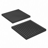
EP4CGX15BF14C8N Altera, EP4CGX15BF14C8N Datasheet - Page 158

EP4CGX15BF14C8N
Manufacturer Part Number
EP4CGX15BF14C8N
Description
IC CYCLONE IV FPGA 15K 169FBGA
Manufacturer
Altera
Series
CYCLONE® IV GXr
Datasheets
1.EP4CGX15BN11C8N.pdf
(44 pages)
2.EP4CGX15BN11C8N.pdf
(14 pages)
3.EP4CGX15BN11C8N.pdf
(478 pages)
4.EP4CGX15BN11C8N.pdf
(10 pages)
Specifications of EP4CGX15BF14C8N
Number Of Logic Elements/cells
14400
Number Of Labs/clbs
900
Total Ram Bits
540000
Number Of I /o
72
Voltage - Supply
1.16 V ~ 1.24 V
Mounting Type
Surface Mount
Operating Temperature
0°C ~ 85°C
Package / Case
169-FBGA
Lead Free Status / RoHS Status
Lead free / RoHS Compliant
Number Of Gates
-
Other names
544-1475
Available stocks
Company
Part Number
Manufacturer
Quantity
Price
Company:
Part Number:
EP4CGX15BF14C8N
Manufacturer:
ALTERA33
Quantity:
276
- EP4CGX15BN11C8N PDF datasheet
- EP4CGX15BN11C8N PDF datasheet #2
- EP4CGX15BN11C8N PDF datasheet #3
- EP4CGX15BN11C8N PDF datasheet #4
- Current page: 158 of 478
- Download datasheet (13Mb)
7–10
Figure 7–6. DQS, CQ, or CQ# Pins for Cyclone IV E Devices in the 144-Pin EQFP and 164-pin MBGA Packages
Optional Parity, DM, and Error Correction Coding Pins
Cyclone IV Device Handbook, Volume 1
Figure 7–6
banks of the Cyclone IV E device in the 144-pin EQFP and 164-pin MBGA packages.
In Cyclone IV devices, the ×9 mode uses the same DQ and DQS pins as the ×8 mode,
and one additional DQ pin that serves as a regular I/O pin in the ×8 mode. The ×18
mode uses the same DQ and DQS pins as ×16 mode, with two additional DQ pins that
serve as regular I/O pins in the ×16 mode. Similarly, the ×36 mode uses the same DQ
and DQS pins as the ×32 mode, with four additional DQ pins that serve as regular I/O
pins in the ×32 mode. When not used as DQ or DQS pins, the memory interface pins
are available as regular I/O pins.
Cyclone IV devices support parity in ×9, ×18, and ×36 modes. One parity bit is
available per eight bits of data pins. You can use any of the DQ pins for parity in
Cyclone IV devices because the parity pins are treated and configured similarly to DQ
pins.
DM pins are only required when writing to DDR2 and DDR SDRAM devices.
QDR II SRAM devices use the BWS# signal to select the byte to be written into
memory. A low signal on the DM or BWS# pin indicates the write is valid. Driving the
DM or BWS# pin high causes the memory to mask the DQ signals. Each group of DQS
and DQ signals has one DM pin. Similar to the DQ output signals, the DM signals are
clocked by the -90° shifted clock.
In Cyclone IV devices, the DM pins are preassigned in the device pinouts. The
Quartus II Fitter treats the DQ and DM pins in a DQS group equally for placement
purposes. The preassigned DQ and DM pins are the preferred pins to use.
DQS1L/CQ1L#
DQS0L/CQ1L
shows the location and numbering of the DQS, DQ, or CQ# pins in I/O
I/O Bank 8
I/O Bank 3
Cyclone IV E Devices
in 144-pin EQFP and
164-pin MBGA
I/O Bank 7
I/O Bank 4
Chapter 7: External Memory Interfaces in Cyclone IV Devices
Cyclone IV Devices Memory Interfaces Pin Support
DQS0R/CQ1R
DQS1R/CQ1R#
© December 2010 Altera Corporation
Related parts for EP4CGX15BF14C8N
Image
Part Number
Description
Manufacturer
Datasheet
Request
R

Part Number:
Description:
CYCLONE II STARTER KIT EP2C20N
Manufacturer:
Altera
Datasheet:

Part Number:
Description:
CPLD, EP610 Family, ECMOS Process, 300 Gates, 16 Macro Cells, 16 Reg., 16 User I/Os, 5V Supply, 35 Speed Grade, 24DIP
Manufacturer:
Altera Corporation
Datasheet:

Part Number:
Description:
CPLD, EP610 Family, ECMOS Process, 300 Gates, 16 Macro Cells, 16 Reg., 16 User I/Os, 5V Supply, 15 Speed Grade, 24DIP
Manufacturer:
Altera Corporation
Datasheet:

Part Number:
Description:
Manufacturer:
Altera Corporation
Datasheet:

Part Number:
Description:
CPLD, EP610 Family, ECMOS Process, 300 Gates, 16 Macro Cells, 16 Reg., 16 User I/Os, 5V Supply, 30 Speed Grade, 24DIP
Manufacturer:
Altera Corporation
Datasheet:

Part Number:
Description:
High-performance, low-power erasable programmable logic devices with 8 macrocells, 10ns
Manufacturer:
Altera Corporation
Datasheet:

Part Number:
Description:
High-performance, low-power erasable programmable logic devices with 8 macrocells, 7ns
Manufacturer:
Altera Corporation
Datasheet:

Part Number:
Description:
Classic EPLD
Manufacturer:
Altera Corporation
Datasheet:

Part Number:
Description:
High-performance, low-power erasable programmable logic devices with 8 macrocells, 10ns
Manufacturer:
Altera Corporation
Datasheet:

Part Number:
Description:
Manufacturer:
Altera Corporation
Datasheet:

Part Number:
Description:
Manufacturer:
Altera Corporation
Datasheet:

Part Number:
Description:
Manufacturer:
Altera Corporation
Datasheet:

Part Number:
Description:
CPLD, EP610 Family, ECMOS Process, 300 Gates, 16 Macro Cells, 16 Reg., 16 User I/Os, 5V Supply, 25 Speed Grade, 24DIP
Manufacturer:
Altera Corporation
Datasheet:


