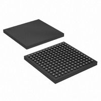
EP4CGX15BF14C8N Altera, EP4CGX15BF14C8N Datasheet - Page 159

EP4CGX15BF14C8N
Manufacturer Part Number
EP4CGX15BF14C8N
Description
IC CYCLONE IV FPGA 15K 169FBGA
Manufacturer
Altera
Series
CYCLONE® IV GXr
Datasheets
1.EP4CGX15BN11C8N.pdf
(44 pages)
2.EP4CGX15BN11C8N.pdf
(14 pages)
3.EP4CGX15BN11C8N.pdf
(478 pages)
4.EP4CGX15BN11C8N.pdf
(10 pages)
Specifications of EP4CGX15BF14C8N
Number Of Logic Elements/cells
14400
Number Of Labs/clbs
900
Total Ram Bits
540000
Number Of I /o
72
Voltage - Supply
1.16 V ~ 1.24 V
Mounting Type
Surface Mount
Operating Temperature
0°C ~ 85°C
Package / Case
169-FBGA
Lead Free Status / RoHS Status
Lead free / RoHS Compliant
Number Of Gates
-
Other names
544-1475
Available stocks
Company
Part Number
Manufacturer
Quantity
Price
Company:
Part Number:
EP4CGX15BF14C8N
Manufacturer:
ALTERA33
Quantity:
276
- EP4CGX15BN11C8N PDF datasheet
- EP4CGX15BN11C8N PDF datasheet #2
- EP4CGX15BN11C8N PDF datasheet #3
- EP4CGX15BN11C8N PDF datasheet #4
- Current page: 159 of 478
- Download datasheet (13Mb)
Chapter 7: External Memory Interfaces in Cyclone IV Devices
Cyclone IV Devices Memory Interfaces Pin Support
Address and Control/Command Pins
Memory Clock Pins
© December 2010 Altera Corporation
f
1
1
Some DDR2 SDRAM and DDR SDRAM devices support error correction coding
(ECC), a method of detecting and automatically correcting errors in data
transmission. In 72-bit DDR2 or DDR SDRAM, there are eight ECC pins and 64 data
pins. Connect the DDR2 and DDR SDRAM ECC pins to a separate DQS or DQ group
in Cyclone IV devices. The memory controller needs additional logic to encode and
decode the ECC data.
The address signals and the control or command signals are typically sent at a single
data rate. You can use any of the user I/O pins on all I/O banks of Cyclone IV devices
to generate the address and control or command signals to the memory device.
Cyclone IV devices do not support QDR II SRAM in the burst length of two.
In DDR2 and DDR SDRAM memory interfaces, the memory clock signals (CK and
CK#) are used to capture the address signals and the control or command signals.
Similarly, QDR II SRAM devices use the write clocks (K and K#) to capture the
address and command signals. The CK/CK# and K/K# signals are generated to
resemble the write-data strobe using the DDIO registers in Cyclone IV devices.
CK/CK# pins must be placed on differential I/O pins (DIFFIO in Pin Planner) and in
the same bank or on the same side as the data pins. You can use either side of the
device for wraparound interfaces. As seen in the Pin Planner Pad View, CK0 cannot be
located in the same row and column pad group as any of the interfacing DQ pins.
For more information about memory clock pin placement, refer to
Pin, and Board Layout Guidelines
of the External Memory Interface Handbook.
Cyclone IV Device Handbook, Volume 1
Volume 2: Device,
7–11
Related parts for EP4CGX15BF14C8N
Image
Part Number
Description
Manufacturer
Datasheet
Request
R

Part Number:
Description:
CYCLONE II STARTER KIT EP2C20N
Manufacturer:
Altera
Datasheet:

Part Number:
Description:
CPLD, EP610 Family, ECMOS Process, 300 Gates, 16 Macro Cells, 16 Reg., 16 User I/Os, 5V Supply, 35 Speed Grade, 24DIP
Manufacturer:
Altera Corporation
Datasheet:

Part Number:
Description:
CPLD, EP610 Family, ECMOS Process, 300 Gates, 16 Macro Cells, 16 Reg., 16 User I/Os, 5V Supply, 15 Speed Grade, 24DIP
Manufacturer:
Altera Corporation
Datasheet:

Part Number:
Description:
Manufacturer:
Altera Corporation
Datasheet:

Part Number:
Description:
CPLD, EP610 Family, ECMOS Process, 300 Gates, 16 Macro Cells, 16 Reg., 16 User I/Os, 5V Supply, 30 Speed Grade, 24DIP
Manufacturer:
Altera Corporation
Datasheet:

Part Number:
Description:
High-performance, low-power erasable programmable logic devices with 8 macrocells, 10ns
Manufacturer:
Altera Corporation
Datasheet:

Part Number:
Description:
High-performance, low-power erasable programmable logic devices with 8 macrocells, 7ns
Manufacturer:
Altera Corporation
Datasheet:

Part Number:
Description:
Classic EPLD
Manufacturer:
Altera Corporation
Datasheet:

Part Number:
Description:
High-performance, low-power erasable programmable logic devices with 8 macrocells, 10ns
Manufacturer:
Altera Corporation
Datasheet:

Part Number:
Description:
Manufacturer:
Altera Corporation
Datasheet:

Part Number:
Description:
Manufacturer:
Altera Corporation
Datasheet:

Part Number:
Description:
Manufacturer:
Altera Corporation
Datasheet:

Part Number:
Description:
CPLD, EP610 Family, ECMOS Process, 300 Gates, 16 Macro Cells, 16 Reg., 16 User I/Os, 5V Supply, 25 Speed Grade, 24DIP
Manufacturer:
Altera Corporation
Datasheet:


