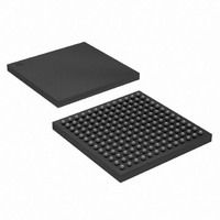
EP4CGX15BF14C8N Altera, EP4CGX15BF14C8N Datasheet - Page 48

EP4CGX15BF14C8N
Manufacturer Part Number
EP4CGX15BF14C8N
Description
IC CYCLONE IV FPGA 15K 169FBGA
Manufacturer
Altera
Series
CYCLONE® IV GXr
Datasheets
1.EP4CGX15BN11C8N.pdf
(44 pages)
2.EP4CGX15BN11C8N.pdf
(14 pages)
3.EP4CGX15BN11C8N.pdf
(478 pages)
4.EP4CGX15BN11C8N.pdf
(10 pages)
Specifications of EP4CGX15BF14C8N
Number Of Logic Elements/cells
14400
Number Of Labs/clbs
900
Total Ram Bits
540000
Number Of I /o
72
Voltage - Supply
1.16 V ~ 1.24 V
Mounting Type
Surface Mount
Operating Temperature
0°C ~ 85°C
Package / Case
169-FBGA
Lead Free Status / RoHS Status
Lead free / RoHS Compliant
Number Of Gates
-
Other names
544-1475
Available stocks
Company
Part Number
Manufacturer
Quantity
Price
Company:
Part Number:
EP4CGX15BF14C8N
Manufacturer:
ALTERA33
Quantity:
276
- EP4CGX15BN11C8N PDF datasheet
- EP4CGX15BN11C8N PDF datasheet #2
- EP4CGX15BN11C8N PDF datasheet #3
- EP4CGX15BN11C8N PDF datasheet #4
- Current page: 48 of 478
- Download datasheet (13Mb)
3–12
Figure 3–11. Cyclone IV Devices True Dual-Port Timing Waveform
Shift Register Mode
Cyclone IV Device Handbook, Volume 1
q_a (asynch)
q_b (asynch)
address_a
address_b
data_a
rden_a
wren_a
wren_b
rden_b
clk_a
clk_b
din-1
an-1
doutn-1
Cyclone IV devices M9K memory blocks can implement shift registers for digital
signal processing (DSP) applications, such as finite impulse response (FIR) filters,
pseudo-random number generators, multi-channel filtering, and auto-correlation and
cross-correlation functions. These and other DSP applications require local data
storage, traditionally implemented with standard flipflops that quickly exhaust many
logic cells for large shift registers. A more efficient alternative is to use embedded
memory as a shift register block, which saves logic cell and routing resources.
The size of a (w × m × n) shift register is determined by the input data width (w), the
length of the taps (m), and the number of taps (n), and must be less than or equal to
the maximum number of memory bits, which is 9,216 bits. In addition, the size of
(w × n) must be less than or equal to the maximum width of the block, which is 36 bits.
If you need a larger shift register, you can cascade the M9K memory blocks.
bn
din-1
din
an
doutn
din
b0
a0
dout0
a1
dout0
dout1
b1
a2
dout2
a3
Chapter 3: Memory Blocks in Cyclone IV Devices
dout3
dout1
b2
din4
a4
© November 2009 Altera Corporation
din4
din5
a5
dout2
din5
b3
din6
a6
Memory Modes
Related parts for EP4CGX15BF14C8N
Image
Part Number
Description
Manufacturer
Datasheet
Request
R

Part Number:
Description:
CYCLONE II STARTER KIT EP2C20N
Manufacturer:
Altera
Datasheet:

Part Number:
Description:
CPLD, EP610 Family, ECMOS Process, 300 Gates, 16 Macro Cells, 16 Reg., 16 User I/Os, 5V Supply, 35 Speed Grade, 24DIP
Manufacturer:
Altera Corporation
Datasheet:

Part Number:
Description:
CPLD, EP610 Family, ECMOS Process, 300 Gates, 16 Macro Cells, 16 Reg., 16 User I/Os, 5V Supply, 15 Speed Grade, 24DIP
Manufacturer:
Altera Corporation
Datasheet:

Part Number:
Description:
Manufacturer:
Altera Corporation
Datasheet:

Part Number:
Description:
CPLD, EP610 Family, ECMOS Process, 300 Gates, 16 Macro Cells, 16 Reg., 16 User I/Os, 5V Supply, 30 Speed Grade, 24DIP
Manufacturer:
Altera Corporation
Datasheet:

Part Number:
Description:
High-performance, low-power erasable programmable logic devices with 8 macrocells, 10ns
Manufacturer:
Altera Corporation
Datasheet:

Part Number:
Description:
High-performance, low-power erasable programmable logic devices with 8 macrocells, 7ns
Manufacturer:
Altera Corporation
Datasheet:

Part Number:
Description:
Classic EPLD
Manufacturer:
Altera Corporation
Datasheet:

Part Number:
Description:
High-performance, low-power erasable programmable logic devices with 8 macrocells, 10ns
Manufacturer:
Altera Corporation
Datasheet:

Part Number:
Description:
Manufacturer:
Altera Corporation
Datasheet:

Part Number:
Description:
Manufacturer:
Altera Corporation
Datasheet:

Part Number:
Description:
Manufacturer:
Altera Corporation
Datasheet:

Part Number:
Description:
CPLD, EP610 Family, ECMOS Process, 300 Gates, 16 Macro Cells, 16 Reg., 16 User I/Os, 5V Supply, 25 Speed Grade, 24DIP
Manufacturer:
Altera Corporation
Datasheet:


