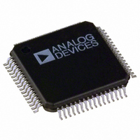
ADE7166ASTZF8 Analog Devices Inc, ADE7166ASTZF8 Datasheet - Page 10

ADE7166ASTZF8
Manufacturer Part Number
ADE7166ASTZF8
Description
IC ENERGY METER 1PHASE 64LQFP
Manufacturer
Analog Devices Inc
Specifications of ADE7166ASTZF8
Applications
Energy Measurement
Core Processor
8052
Program Memory Type
FLASH (8 kB)
Controller Series
ADE71xx
Ram Size
512 x 8
Interface
I²C, SPI, UART
Number Of I /o
20
Voltage - Supply
3.135 V ~ 3.465 V
Operating Temperature
-40°C ~ 85°C
Mounting Type
Surface Mount
Package / Case
64-LQFP
Ic Function
Single Phase Energy Measurement IC
Supply Voltage Range
3.13V To 3.46V, 2.4V To 3.7V
Operating Temperature Range
-40°C To +85°C
Digital Ic Case Style
LQFP
No. Of Pins
64
Lead Free Status / RoHS Status
Lead free / RoHS Compliant
Available stocks
Company
Part Number
Manufacturer
Quantity
Price
Company:
Part Number:
ADE7166ASTZF8
Manufacturer:
Analog Devices Inc
Quantity:
10 000
Company:
Part Number:
ADE7166ASTZF8-RL
Manufacturer:
Analog Devices Inc
Quantity:
10 000
ADE7566/ADE7569/ADE7166/ADE7169
TIMING SPECIFICATIONS
AC inputs during testing were driven at V
and 0.45 V for Logic 0. Timing measurements were made at V
minimum for Logic 1 and V
Figure 3.
For timing purposes, a port pin is no longer floating when a
100 mV change from load voltage occurs. A port pin begins to
Table 5. Clock Input (External Clock Driven XTAL1) Parameter
Parameter
t
t
t
t
t
1/t
1
Table 6. I
Parameter
t
t
t
t
t
t
t
t
t
t
t
1
CK
CKL
CKH
CKR
CKF
BUF
L
H
SHD
DSU
DHD
RSU
PSU
R
F
SUP
The ADE7566/ADE7569/ADE7166/ADE7169 internal PLL locks onto a multiple (512 times) of the 32.768 kHz external crystal frequency to provide a stable 4.096 MHz
Input filtering on both the SCLK and SDATA inputs suppresses noise spikes less than 50 ns.
internal clock for the system. The core can operate at this frequency or at a binary submultiple defined by the CD[2:0] bits, selected via the POWCON SFR (see Table 25).
CORE
1
2
SDATA (I/O)
C-Compatible Interface Timing Parameters (400 kHz)
SCLK (I)
V
t
PSU
SWOUT
Description
Bus-free time between stop condition and start condition
SCLK low pulse width
SCLK high pulse width
Start condition hold time
Data setup time
Data hold time
Setup time for repeated start
Stop condition setup time
Rise time of both SCLK and SDATA
Fall time of both SCLK and SDATA
Pulse width of spike suppressed
CONDITION
– 0.5V
0.45V
STOP
Description
XTAL1 period
XTAL1 width low
XTAL1 width high
XTAL1 rise time
XTAL1 fall time
Core clock frequency
PS
IL
maximum for Logic 0, as shown in
t
BUF
CONDITION
START
t
DSU
0.2V
0.2V
SWOUT
TEST POINTS
t
SWOUT
SHD
SWOUT
− 0.5 V for Logic 1
1
MSB
1
– 0.1V
+ 0.9V
Figure 3. Timing Waveform Characteristics
Figure 4. I
t
DHD
2 TO 7
IH
2
Rev. A | Page 10 of 144
C-Compatible Interface Timing
t
L
V
LOAD
0.032768
Min
LSB
V
V
8
LOAD
LOAD
t
t
SUP
SUP
float when a 100 mV change from the loaded V
occurs as shown in Figure 3.
C
to 3.6 V; all specifications T
LOAD
– 0.1V
+ 0.1V
t
H
t
DSU
for all outputs = 80 pF, unless otherwise noted. V
32.768 kHz External Crystal
ACK
REFERENCE
9
POINTS
TIMING
t
RSU
Typ
30.52
6.26
6.26
9
9
1.024
t
DHD
REPEATED
START
S(R)
MIN
to T
V
V
LOAD
LOAD
MAX
– 0.1V
– 0.1V
Max
4.096
, unless otherwise noted.
t
F
MSB
t
V
Typ
1.36
1.14
251.35
740
400
12.5
400
1.3
200
300
50
F
LOAD
1
t
R
t
R
OH
/V
OL
DD
Unit
μs
μs
μs
ns
ns
MHz
level
= 2.7 V
μs
ns
ns
ns
ns
Unit
μs
μs
μs
ns
ns
ns


