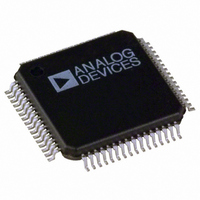
ADE7166ASTZF8 Analog Devices Inc, ADE7166ASTZF8 Datasheet - Page 100

ADE7166ASTZF8
Manufacturer Part Number
ADE7166ASTZF8
Description
IC ENERGY METER 1PHASE 64LQFP
Manufacturer
Analog Devices Inc
Specifications of ADE7166ASTZF8
Applications
Energy Measurement
Core Processor
8052
Program Memory Type
FLASH (8 kB)
Controller Series
ADE71xx
Ram Size
512 x 8
Interface
I²C, SPI, UART
Number Of I /o
20
Voltage - Supply
3.135 V ~ 3.465 V
Operating Temperature
-40°C ~ 85°C
Mounting Type
Surface Mount
Package / Case
64-LQFP
Ic Function
Single Phase Energy Measurement IC
Supply Voltage Range
3.13V To 3.46V, 2.4V To 3.7V
Operating Temperature Range
-40°C To +85°C
Digital Ic Case Style
LQFP
No. Of Pins
64
Lead Free Status / RoHS Status
Lead free / RoHS Compliant
Available stocks
Company
Part Number
Manufacturer
Quantity
Price
Company:
Part Number:
ADE7166ASTZF8
Manufacturer:
Analog Devices Inc
Quantity:
10 000
Company:
Part Number:
ADE7166ASTZF8-RL
Manufacturer:
Analog Devices Inc
Quantity:
10 000
ADE7566/ADE7569/ADE7166/ADE7169
BLINK MODE
Blink mode is enabled by setting the BLINKEN bit in the LCD
Configuration SFR (LCDCON, 0x95). This mode is used to
alternate between the LCD on state and LCD off state so that
the LCD screen appears to blink. There are two blinking modes:
a software controlled blink mode and an automatic blink mode.
Software Controlled Blink Mode
The LCD blink rate can be controlled by user code with the
BLKMOD[1:0] bits in the LCD Clock SFR (LCDCLK, 0x96) by
toggling the bits to turn the display on and off at a rate
determined by the MCU code.
Automatic Blink Mode
There are five blink rates available if the RTC peripheral is
enabled by setting the RTCEN bit in the RTC Configuration
SFR (TIMECON, 0xA1). These blink rates are selected by the
BLKMOD[1:0] and BLKFREQ[1:0] bits in the LCD Clock SFR
(LCDCLK, 0x96); see Table 82.
DISPLAY ELEMENT CONTROL
A bank of 15 bytes of data memory located in the LCD module
controls the on or off state of each LCD segment. The LCD data
memory is stored in Address 0 through Address 14 in the LCD
module. Each byte configures the on and off states of two segment
lines. The LSBs store the state of the even numbered segment
lines, and the MSBs store the state of the odd numbered segment
lines. For example, LCD Data Address 0 refers to segment lines
one and zero (see Table 89). Note that the LCD data memory is
maintained in PSM2 operating mode.
The LCD data memory is accessed indirectly through the LCD
Pointer SFR (LCDPTR, 0xAC) and LCD Data SFR (LCDDAT,
0xAE). Moving a value to the LCDPTR SFR selects the LCD
Table 89. LCD Data Memory Accessed Indirectly Through LCD Pointer SFR (LCDPTR, 0xAC) and LCD Data SFR (LCDDAT, 0xAE)
LCD Memory Address
0x0E
0x0D
0x0C
0x0B
0x0A
0x09
0x08
0x07
0x06
0x05
0x04
0x03
0x02
0x01
0x00
1
2
COMx designates the common lines.
FPx designates the segment lines.
COM3
FP27
FP25
FP23
FP21
FP19
FP17
FP15
FP13
FP11
FP9
FP7
FP5
FP3
FP1
LCD Pointer SFR (LCDPTR, 0xAC)
COM2
FP27
FP25
FP23
FP21
FP19
FP17
FP15
FP13
FP11
FP9
FP7
FP5
FP3
FP1
COM1
FP27
FP25
FP23
FP21
FP19
FP17
FP15
FP13
FP11
FP9
FP7
FP5
FP3
FP1
Rev. A | Page 100 of 144
COM0
FP27
FP25
FP23
FP21
FP19
FP17
FP15
FP13
FP11
FP9
FP7
FP5
FP3
FP1
data byte to be accessed and initiates a read or write operation
(see Table 86).
Writing to LCD Data Registers
To update the LCD data memory, first set the LSB of the LCD
Configuration Y SFR (LCDCONY, 0xB1) to freeze the data
being displayed on the LCD while updating it. Then, move the
data to the LCD Data SFR (LCDDAT, 0xAE) prior to accessing
the LCD Pointer SFR (LCDPTR, 0xAC). When the MSB of the
LCDPTR SFR is set, the content of the LCDDAT SFR is
transferred to the internal LCD data memory designated by the
address in the LCDPTR SFR. Clear the LSB of the LCD
Configuration Y SFR (LCDCONY, 0xB1) when all of the data
memory has been updated to allow the use of the new LCD
setup for display.
To update the segments attached to the FP10 and FP11 pins, use
the following sample 8052 code:
ORL
MOV
MOV
ANL
Reading LCD Data Registers
When the MSB of the LCD Pointer SFR (LCDPTR, 0xAC) is
cleared, the content of the LCD data memory address designated by
LCDPTR is transferred to the LCD Data SFR (LCDDAT, 0xAE).
Sample 8052 code to read the contents of LCD Data Memory
Address 0x07, which holds the on and off state of the segments
attached to FP14 and FP15, is as follows.
MOV
MOV
LCDCONY,#01h ;start updating the data
LCDDATA,#FFh
LCDPTR,#80h OR 05h
LCDCONY,#0FEh ;update finished
LCDPTR,#07h
R1, LCDDATA
COM3
FP28
FP26
FP24
FP22
FP20
FP18
FP16
FP14
FP12
FP10
FP8
FP6
FP4
FP2
FP0
LCD Pointer SFR (LCDDAT, 0xAE)
COM2
FP28
FP26
FP24
FP22
FP20
FP18
FP16
FP14
FP12
FP10
FP8
FP6
FP4
FP2
FP0
COM1
FP28
FP26
FP24
FP22
FP20
FP18
FP16
FP14
FP12
FP10
FP8
FP6
FP4
FP2
FP0
COM0
FP28
FP26
FP24
FP22
FP20
FP18
FP16
FP14
FP12
FP10
FP8
FP6
FP4
FP2
FP0
1, 2


