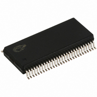
CY7C66113-PVC Cypress Semiconductor Corp, CY7C66113-PVC Datasheet - Page 11

CY7C66113-PVC
Manufacturer Part Number
CY7C66113-PVC
Description
IC MCU 8K USB HUB 4 PORT 56TSSOP
Manufacturer
Cypress Semiconductor Corp
Specifications of CY7C66113-PVC
Applications
USB Hub/Microcontroller
Core Processor
M8
Program Memory Type
OTP (8 kB)
Controller Series
USB Hub
Ram Size
256 x 8
Interface
I²C, USB, HAPI
Number Of I /o
31
Voltage - Supply
4 V ~ 5.5 V
Operating Temperature
0°C ~ 70°C
Mounting Type
Surface Mount
Package / Case
56-SSOP
Operating Temperature (max)
70C
Operating Temperature (min)
0C
Operating Temperature Classification
Commercial
Mounting
Surface Mount
Pin Count
56
Lead Free Status / RoHS Status
Contains lead / RoHS non-compliant
For Use With
CY3649 - PROGRAMMER HI-LO USB M8428-1339 - KIT LOW SPEED PERSONALITY BOARD
Lead Free Status / RoHS Status
Not Compliant, Contains lead / RoHS non-compliant
Other names
428-1330
Available stocks
Company
Part Number
Manufacturer
Quantity
Price
Company:
Part Number:
CY7C66113-PVC
Manufacturer:
CY
Quantity:
10
4.0
4.1
Table 4-1. Pin Assignments
4.2
I/O registers are accessed via the I/O Read (IORD) and I/O Write (IOWR, IOWX) instructions. IORD reads data from the selected
port into the accumulator. IOWR performs the reverse; it writes data from the accumulator to the selected port. Indexed I/O Write
(IOWX) adds the contents of X to the address in the instruction to form the port address and writes data from the accumulator to
the specified port. Specifying address 0 (e.g., IOWX 0h) means the I/O register is selected solely by the contents of X.
All undefined registers are reserved. It is important not to write to reserved registers as this may cause an undefined operation
or increased current consumption during operation. When writing to registers with reserved bits, the reserved bits must be written
with ‘0.’
Table 4-2. I/O Register Summary
Document #: 38-08024 Rev. *A
D+[0], D–[0]
D+[1], D–[1]
D+[2], D–[2]
D+[3], D–[3]
D+[4], D–[4]
P0[7:0]
P1[7:0]
P2[7:0]
P3[6:0]
DAC[7:0]
XTAL
XTAL
V
V
GND
V
Port 0 Data
Port 1 Data
Port 2 Data
Port 3 Data
Port 0 Interrupt Enable
Port 1 Interrupt Enable
Port 2 Interrupt Enable
Port 3 Interrupt Enable
GPIO Configuration
PP
CC
REF
Name
IN
OUT
Register Name
Pin Assignments
I/O Register Summary
Product Summary Tables
I/O
I/O
I/O
I/O
I/O
I/O
I/O
I/O
I/O
I/O
IN
OUT
IN
I/O
8, 9
12, 13
15, 16
40, 41
35, 36
21, 25, 22, 26,
23, 27, 24, 28
6, 43, 5, 44, 4,
45, 47, 46
19, 30, 18, 31,
17, 33, 14, 34
37, 10, 39, 7, 42 43, 12, 46, 10,
n/a
2
1
29
48
11, 20, 32, 38
3
48-Pin
0x00
0x01
0x02
0x03
0x04
0x05
0x06
0x07
0x08
I/O Address
8, 9
13, 14
16, 17
48, 49
44, 45
22, 32, 23, 33,
24, 34, 25, 35
6, 51, 5, 52, 4,
53, 55, 54
20, 38, 19, 39,
18, 41, 15, 42
47, 7, 50
21, 29, 26, 30,
27, 31, 28, 37
2
1
36
56
11, 40
3
56-Pin
R/W
R/W
R/W
R/W
W
W
W
W
R/W
Read/Write
Upstream port, USB differential data.
Downstream port 1, USB differential data.
Downstream port 2, USB differential data.
Downstream port 3, USB differential data.
Downstream port 4, USB differential data.
GPIO Port 0.
GPIO Port 1.
GPIO Port 2.
GPIO Port 3, capable of sinking 12 mA (typical).
Digital to Analog Converter (DAC) Port with programmable current
sink outputs. DAC[1:0] offer a programmable range of 3.2 to 16 mA
typical. DAC[7:2] have a programmable sink current range of 0.2 to 1.0
mA typical.
6-MHz crystal or external clock input.
6-MHz crystal out.
Programming voltage supply, tie to ground during normal
operation.
Voltage supply.
Ground.
External 3.3V supply voltage for the differential data output buffers
and the D+ pull-up.
GPIO Port 0 Data
GPIO Port 1 Data
GPIO Port 2 Data
GPIO Port 3 Data
Interrupt Enable for Pins in Port 0
Interrupt Enable for Pins in Port 1
Interrupt Enable for Pins in Port 2
Interrupt Enable for Pins in Port 3
GPIO Port Configurations
Description
Function
CY7C66013
CY7C66113
Page 11 of 58
20
20
20
20
21
22
22
22
20
Page


