CY7C66113-PVC Cypress Semiconductor Corp, CY7C66113-PVC Datasheet - Page 24
CY7C66113-PVC
Manufacturer Part Number
CY7C66113-PVC
Description
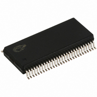
IC MCU 8K USB HUB 4 PORT 56TSSOP
Manufacturer
Cypress Semiconductor Corp
Specifications of CY7C66113-PVC
Applications
USB Hub/Microcontroller
Core Processor
M8
Program Memory Type
OTP (8 kB)
Controller Series
USB Hub
Ram Size
256 x 8
Interface
I²C, USB, HAPI
Number Of I /o
31
Voltage - Supply
4 V ~ 5.5 V
Operating Temperature
0°C ~ 70°C
Mounting Type
Surface Mount
Package / Case
56-SSOP
Operating Temperature (max)
70C
Operating Temperature (min)
0C
Operating Temperature Classification
Commercial
Mounting
Surface Mount
Pin Count
56
Lead Free Status / RoHS Status
Contains lead / RoHS non-compliant
For Use With
CY3649 - PROGRAMMER HI-LO USB M8428-1339 - KIT LOW SPEED PERSONALITY BOARD
Lead Free Status / RoHS Status
Not Compliant, Contains lead / RoHS non-compliant
Other names
428-1330
Available stocks
Company
Part Number
Manufacturer
Quantity
Price
Company:

Part Number:
CY7C66113-PVC
Manufacturer:
CY
Quantity:
10


Bit [7..0]: Enable bit x (x= 0..7)
11.0
The 12-bit timer operates with a 1- s tick, provides two interrupts (128 s and 1.024 ms) and allows the firmware to directly time
events that are up to 4 ms in duration. The lower eight bits of the timer can be read directly by the firmware. Reading the lower
8 bits latches the upper four bits into a temporary register. When the firmware reads the upper four bits of the timer, it is actually
reading the count stored in the temporary register. The effect of this is to ensure a stable 12-bit timer value can be read, even
when the two reads are separated in time.
Bit [7:0]: Timer lower eight bits
Timer MSB
Bit [3:0]: Timer higher nibble
Bit [7:4]: Reserved
12.0
Internal hardware supports communication with external devices through two interfaces: a two-wire I
for 1, 2, or 3 byte transfers. The I
common configuration register (see Figure 12-1)
I
Document #: 38-08024 Rev. *A
Reset
Timer LSB
2
Bit #
Bit Name
Read/Write
Reset
Bit #
Bit Name
Read/Write
Reset
Bit #
Bit Name
Read/Write
C Configuration
1= Selects positive polarity (rising edge) that causes an interrupt (if enabled);
0= Selects negative polarity (falling edge) that causes an interrupt (if enabled).
12-bit Free-running Timer
I
2
C and HAPI Configuration Register
0
7
Timer Bit 7
R
0
7
Reserved
-
0
7
I
R/W
2
C Position
11
L
D3 D2 D1 D0 D7 D6 D5 D4 D3 D2 D1 D0
10 9
L2
0
6
Timer Bit 6
R
0
6
Reserved
-
0
6
Reserved
-
L1 L0
2
C-compatible and HAPI functions, discussed in detail in Sections 13.0 and 14.0, share a
8
Figure 12-1. HAPI/I
7
Figure 10-5. DAC Port Interrupt Polarity
0
5
Timer Bit 5
R
0
5
Reserved
-
0
5
LEMPTY
Polarity
R/W
Figure 11-3. Timer Block Diagram
Figure 11-1. Timer LSB Register
6
[3]
Figure 11-2.
. All bits of this register are cleared on reset.
5
0
4
Timer Bit 4
R
0
4
Reserved
-
0
4
DRDY
Polarity
R/W
4
2
C Configuration Register
Timer MSB Register
3
2
0
3
Timer Bit 3
R
0
3
Timer Bit 11
R
0
3
Latch
Empty
R
1
0
8
2
Timer Bit 2
R
0
2
R
0
2
Data
Ready
R
0
Timer Bit 10
1.024-ms interrupt
128- s interrupt
1 MHz clock
To Timer Registers
1
Timer Bit 1
R
0
1
Timer Bit 9
R
0
1
HAPI Port
Width Bit 1
R/W
0
2
C-compatible, and a HAPI
CY7C66013
CY7C66113
Page 24 of 58
0
Timer Bit 0
R
0
0
Timer Bit 8
R
0
0
HAPI Port
Width Bit 0
R/W
0
ADDRESS 0x24
ADDRESS 0x25
ADDRESS 0x09
Related parts for CY7C66113-PVC
Image
Part Number
Description
Manufacturer
Datasheet
Request
R

Part Number:
Description:
Manufacturer:
Cypress Semiconductor Corp
Datasheet:
Part Number:
Description:
Manufacturer:
Cypress Semiconductor Corp
Datasheet:
Part Number:
Description:
Manufacturer:
Cypress Semiconductor Corp
Datasheet:
Part Number:
Description:
Manufacturer:
Cypress Semiconductor Corp
Datasheet:
Part Number:
Description:
Manufacturer:
Cypress Semiconductor Corp
Datasheet: