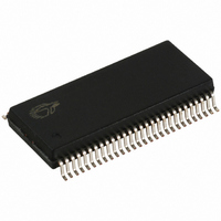
CY7C66113-PVC Cypress Semiconductor Corp, CY7C66113-PVC Datasheet - Page 32

CY7C66113-PVC
Manufacturer Part Number
CY7C66113-PVC
Description
IC MCU 8K USB HUB 4 PORT 56TSSOP
Manufacturer
Cypress Semiconductor Corp
Specifications of CY7C66113-PVC
Applications
USB Hub/Microcontroller
Core Processor
M8
Program Memory Type
OTP (8 kB)
Controller Series
USB Hub
Ram Size
256 x 8
Interface
I²C, USB, HAPI
Number Of I /o
31
Voltage - Supply
4 V ~ 5.5 V
Operating Temperature
0°C ~ 70°C
Mounting Type
Surface Mount
Package / Case
56-SSOP
Operating Temperature (max)
70C
Operating Temperature (min)
0C
Operating Temperature Classification
Commercial
Mounting
Surface Mount
Pin Count
56
Lead Free Status / RoHS Status
Contains lead / RoHS non-compliant
For Use With
CY3649 - PROGRAMMER HI-LO USB M8428-1339 - KIT LOW SPEED PERSONALITY BOARD
Lead Free Status / RoHS Status
Not Compliant, Contains lead / RoHS non-compliant
Other names
428-1330
Available stocks
Company
Part Number
Manufacturer
Quantity
Price
Company:
Part Number:
CY7C66113-PVC
Manufacturer:
CY
Quantity:
10
16.5
There are five USB endpoint interrupts, one per endpoint. A USB endpoint interrupt is generated after the USB host writes to a
USB endpoint FIFO or after the USB controller sends a packet to the USB host. The interrupt is generated on the last packet of
the transaction (e.g. on the host’s ACK during an IN, or on the device ACK during on OUT). If no ACK is received during an IN
transaction, no interrupt is generated.
16.6
A USB hub interrupt is generated by the hardware after a connect/disconnect change, babble, or a resume event is detected by
the USB repeater hardware. The babble and resume events are additionally gated by the corresponding bits of the Hub Port
Enable Register (Figure 18-3). The connect/disconnect event on a port does not generate an interrupt if the SIE does not drive
the port (i.e., the port is being forced).
16.7
Each DAC I/O pin can generate an interrupt, if enabled. The interrupt polarity for each DAC I/O pin is programmable. A positive
polarity is a rising edge input while a negative polarity is a falling edge input. All of the DAC pins share a single interrupt vector,
which means the firmware needs to read the DAC port to determine which pin or pins caused an interrupt.
If one DAC pin has triggered an interrupt, no other DAC pins can cause a DAC interrupt until that pin has returned to its inactive
(non-trigger) state or the corresponding interrupt enable bit is cleared. The USB Controller does not assign interrupt priority to
different DAC pins and the DAC Interrupt Enable Register is not cleared during the interrupt acknowledge process.
16.8
Each of the GPIO pins can generate an interrupt, if enabled. The interrupt polarity can be programmed for each GPIO port as
part of the GPIO configuration. All of the GPIO pins share a single interrupt vector, which means the firmware needs to read the
GPIO ports with enabled interrupts to determine which pin or pins caused an interrupt. A block diagram of the GPIO interrupt
logic is shown in Figure 16-4. Refer to Sections 9.1 and 9.2 for more information about setting GPIO interrupt polarity and enabling
individual GPIO interrupts.
If one port pin has triggered an interrupt, no other port pins can cause a GPIO interrupt until that port pin has returned to its inactive
(non-trigger) state or its corresponding port interrupt enable bit is cleared. The USB Controller does not assign interrupt priority
to different port pins and the Port Interrupt Enable Registers are not cleared during the interrupt acknowledge process.
When HAPI is enabled, the HAPI logic takes over the interrupt vector and blocks any interrupt from the GPIO bits, including
ports/bits not being used by HAPI. Operation of the HAPI interrupt is independent of the GPIO specific bit interrupt enables, and
is enabled or disabled only by bit 5 of the Global Interrupt Enable Register (0x20) when HAPI is enabled. The settings of the
GPIO bit interrupt enables on ports/bits not used by HAPI still effect the CMOS mode operation of those ports/bits. The effect of
modifying the interrupt bits while the Port Config bits are set to “10” is shown in Table 9-1. The events that generate HAPI interrupts
are described in Section 14.0.
Document #: 38-08024 Rev. *A
GPIO
Pin
IRA
1 = Enable
0 = Disable
USB Endpoint Interrupts
USB Hub Interrupt
DAC Interrupt
GPIO/HAPI Interrupt
Port Interrupt
Enable Register
Configuration
Register
M
U
X
Port
Figure 16-4. GPIO Interrupt Structure
1 = Enable
0 = Disable
(1 input per
GPIO pin)
OR Gate
(Bit 5, Register 0x20)
GPIO Interrupt
Global
Enable
1
GPIO Interrupt
Flip Flop
D
CLR
Q
Interrupt
Encoder
Priority
CY7C66013
CY7C66113
Page 32 of 58
Interrupt
IRQout
Vector


