CY7C66113-PVC Cypress Semiconductor Corp, CY7C66113-PVC Datasheet - Page 26
CY7C66113-PVC
Manufacturer Part Number
CY7C66113-PVC
Description
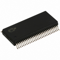
IC MCU 8K USB HUB 4 PORT 56TSSOP
Manufacturer
Cypress Semiconductor Corp
Specifications of CY7C66113-PVC
Applications
USB Hub/Microcontroller
Core Processor
M8
Program Memory Type
OTP (8 kB)
Controller Series
USB Hub
Ram Size
256 x 8
Interface
I²C, USB, HAPI
Number Of I /o
31
Voltage - Supply
4 V ~ 5.5 V
Operating Temperature
0°C ~ 70°C
Mounting Type
Surface Mount
Package / Case
56-SSOP
Operating Temperature (max)
70C
Operating Temperature (min)
0C
Operating Temperature Classification
Commercial
Mounting
Surface Mount
Pin Count
56
Lead Free Status / RoHS Status
Contains lead / RoHS non-compliant
For Use With
CY3649 - PROGRAMMER HI-LO USB M8428-1339 - KIT LOW SPEED PERSONALITY BOARD
Lead Free Status / RoHS Status
Not Compliant, Contains lead / RoHS non-compliant
Other names
428-1330
Available stocks
Company
Part Number
Manufacturer
Quantity
Price
Company:

Part Number:
CY7C66113-PVC
Manufacturer:
CY
Quantity:
10


The I
Table 13-1. I
Bit 7 : MSTR Mode
Bit 6 : Continue/Busy
Bit 5 : Xmit Mode
Bit 4 : ACK
Bit 3 : Addr
Document #: 38-08024 Rev. *A
0
1
2
3
4
5
6
7
Bit Name
Read/Write
Reset
Bit
2
Setting this bit to 1 causes the I
transmitting the first data byte from the data register (this typically holds the target address and R/W bit). Subsequent bytes
are initiated by setting the Continue bit, as described below.
Clearing this bit (set to 0) causes the GPIO pins to operate normally
In master mode, the I
transmit or receive state. The I
event of a loss of arbitration, this MSTR bit is cleared, the ARB Lost bit is set, and an interrupt is generated by the
microcontroller. If the chip is the target of an external master that wins arbitration, then the interrupt is held off until the
transaction from the external master is completed.
When MSTR Mode is cleared from 1 to 0 by a firmware write, an I
This bit is written by the firmware to indicate that the firmware is ready for the next byte transaction to begin. In other words,
the bit has responded to an interrupt request and has completed the required update or read of the data register. During a
read this bit indicates if the hardware is busy and is locking out additional writes to the I
locking allows the hardware to complete certain operations that may require an extended period of time. Following an I
interrupt, the I
firmware to make one control register write without the need to check the Busy bit.
This bit is set by firmware to enter transmit mode and perform a data transmit in master or slave mode. Clearing this bit
sets the part in receive mode. Firmware generally determines the value of this bit from the R/W bit associated with the I
address packet. The Xmit Mode bit state is ignored when initially writing the MSTR Mode or the Restart bits, as these cases
always cause transmit mode for the first byte.
This bit is set or cleared by firmware during receive operation to indicate if the hardware should generate an ACK signal
on the I
time. During transmits (Xmit Mode = 1), this bit should be cleared.
C Status and Control register bits are defined in Table 14-1, with a more detailed description following.
I
Received Stop
ARB Lost/Restart Reads 1 to indicate master has lost arbitration. Reads 0 otherwise.
Addr
ACK
Xmit Mode
Continue/Busy
MSTR Mode
2
C Enable
2
2
C Status and Control Register Bit Definitions
C-compatible bus. Writing a 1 to this bit generates an ACK (SDA LOW) on the I
MSTR Mode
R/W
0
Name
2
C-compatible block does not return to the Busy state until firmware sets the Continue bit. This allows the
2
C-compatible block generates the clock (SCK), and drives the data line as required depending on
Continue/Busy Xmit Mode
R/W
0
When set to ‘1’, the I
normally.
Reads 1 only in slave receive mode, when I
last transaction).
Write to 1 in master mode to perform a restart sequence (also set Continue bit).
Reads 1 during first byte after start/restart in slave mode, or if master loses arbitration.
Reads 0 otherwise. This bit should always be written as 0.
In receive mode, write 1 to generate ACK, 0 for no ACK.
In transmit mode, reads 1 if ACK was received, 0 if no ACK received.
Write to 1 for transmit mode, 0 for receive mode.
Write 1 to indicate ready for next transaction.
Reads 1 when I
Write to 1 for master mode, 0 for slave mode. This bit is cleared if master loses arbitration.
Clearing from 1 to 0 generates Stop bit.
2
C-compatible block performs any required arbitration and clock synchronization. IN the
2
Figure 13-2. I
C-compatible block to initiate a master mode transaction by sending a start bit and
R/W
0
2
C-compatible block is busy with a transaction, 0 when transaction is complete.
2
C-compatible function is enabled. When cleared, I
2
C Status and Control Register
ACK
R/W
0
Addr
R/W
0
2
Description
C Stop bit is generated.
2
C Stop bit detected (unless firmware did not ACK the
Lost/Restart
R/W
0
ARB
2
C Status and Control register. This
2
C-compatible bus at the ACK bit
Received Stop
R/W
0
2
C GPIO pins operate
CY7C66013
CY7C66113
Page 26 of 58
I
R/W
0
2
C Enable
2
2
C
C
Related parts for CY7C66113-PVC
Image
Part Number
Description
Manufacturer
Datasheet
Request
R

Part Number:
Description:
Manufacturer:
Cypress Semiconductor Corp
Datasheet:
Part Number:
Description:
Manufacturer:
Cypress Semiconductor Corp
Datasheet:
Part Number:
Description:
Manufacturer:
Cypress Semiconductor Corp
Datasheet:
Part Number:
Description:
Manufacturer:
Cypress Semiconductor Corp
Datasheet:
Part Number:
Description:
Manufacturer:
Cypress Semiconductor Corp
Datasheet: