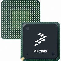
MPC855TCVR50D4 Freescale Semiconductor, MPC855TCVR50D4 Datasheet - Page 11

MPC855TCVR50D4
Manufacturer Part Number
MPC855TCVR50D4
Description
IC MPU POWERQUICC 50MHZ 357PBGA
Manufacturer
Freescale Semiconductor
Datasheets
1.MPC855TVR50D4.pdf
(15 pages)
2.MPC8555ECVTALF.pdf
(88 pages)
3.MPC855TCVR50D4.pdf
(80 pages)
Specifications of MPC855TCVR50D4
Processor Type
MPC8xx PowerQUICC 32-Bit
Speed
50MHz
Voltage
3.3V
Mounting Type
Surface Mount
Package / Case
357-PBGA
Processor Series
MPC8xx
Core
MPC8xx
Data Bus Width
32 bit
Maximum Clock Frequency
50 MHz
Operating Supply Voltage
2.5 V, 3.3 V
Maximum Operating Temperature
+ 95 C
Mounting Style
SMD/SMT
Minimum Operating Temperature
- 40 C
Family Name
MPC8xx
Device Core
PowerQUICC
Device Core Size
32b
Frequency (max)
50MHz
Instruction Set Architecture
RISC
Supply Voltage 1 (typ)
2.5/3.3V
Operating Supply Voltage (max)
3.465/3.6V
Operating Supply Voltage (min)
2/3.135V
Operating Temp Range
-40C to 95C
Operating Temperature Classification
Industrial
Mounting
Surface Mount
Pin Count
357
Package Type
BGA
Lead Free Status / RoHS Status
Lead free / RoHS Compliant
Features
-
Lead Free Status / Rohs Status
Lead free / RoHS Compliant
Available stocks
Company
Part Number
Manufacturer
Quantity
Price
Company:
Part Number:
MPC855TCVR50D4
Manufacturer:
FREESCAL
Quantity:
246
Company:
Part Number:
MPC855TCVR50D4
Manufacturer:
Freescale Semiconductor
Quantity:
10 000
Company:
Part Number:
MPC855TCVR50D4R2
Manufacturer:
Freescale Semiconductor
Quantity:
10 000
Figure 2
The MPC8555E core voltage must always be provided at nominal 1.2 V (see
recommended core voltage). Voltage to the processor interface I/Os are provided through separate sets of
supply pins and must be provided at the voltages shown in
respect to the associated I/O supply voltage. OV
circuits and satisfy appropriate LVCMOS type specifications. The DDR SDRAM interface uses a
single-ended differential receiver referenced the externally supplied MV
GV
Freescale Semiconductor
DD
/2) as is appropriate for the SSTL2 electrical signaling standard.
MPC8555E PowerQUICC™ III Integrated Communications Processor Hardware Specification, Rev. 4.2
shows the undershoot and overshoot voltages at the interfaces of the MPC8555E.
V
V
Note:
IH
1. Note that t
IL
Figure 2. Overshoot/Undershoot Voltage for GV
G/L/OV
G/L/OV
GND – 0.3 V
GND – 0.7 V
G/L/OV
DD
DD
SYS
+ 20%
+ 5%
GND
refers to the clock period associated with the SYSCLK signal.
DD
DD
and LV
Not to Exceed 10%
Table
of t
DD
SYS
based receivers are simple CMOS I/O
2. The input voltage threshold scales with
1
DD
/OV
REF
DD
signal (nominally set to
/LV
Table 2
DD
Electrical Characteristics
for actual
11


